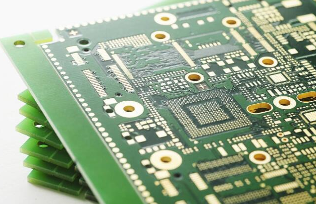
PCB factories often find that some customers' designs do not meet the feasibility requirements of the PCB production process when receiving orders, processing engineering materials and production processes. Of course, this is not to say that the level of designers is limited, but because most PCB design engineers have not been to the PCB factory to understand how a qualified PCB board is produced, and they know too little about PCB production, which leads to the design. There is no way to process and produce the board or the main reason for the problems in the production process, so I hope the following content can provide help for engineers engaged in PCB design.
In order to meet the feasibility requirements of PCB production process, PCB design engineers need to know the following relevant PCB design parameter information:
1. Line
1. Minimum line width: 6mil (0.153mm). That is to say, if the line width is less than 6mil, the production will not be possible (the minimum line width and line spacing of the inner layer of the multilayer board is 8MIL) If the design conditions permit, the larger the design, the better, the larger the line width, the better the factory, the higher the yield, The general design convention is about 10mil, this point is very important, PCB design engineers must consider.

2. Minimum line spacing: 6mil (0.153mm). The minimum line distance is line-to-line, and the line-to-pad distance is not less than 6mil. From the perspective of production, the larger the better, the general rule is 10mil. Of course, the larger the better when the design conditions are possible. This is very important. PCB Design engineers must consider.
3. The distance between the line and the outline line is 0.508mm (20mil)
Second, PCB via via (commonly known as conductive hole)
1. Minimum aperture: 0.3mm (12mil)
2. The minimum via hole (VIA) aperture is not less than 0.3mm (12mil), and the single side of the pad cannot be less than 6mil (0.153mm), preferably greater than 8mil (0.2mm), there is no limit. This is very important, PCB design engineer Must be considered.
3. The via hole (VIA) hole-to-hole spacing (hole edge to hole edge) cannot be less than 6mil, preferably greater than 8mil. This point is very important, and PCB design engineers must consider it.
4. The distance between the pad and the outline line is 0.508mm (20mil)
Three, PAD pad (commonly known as plug-in hole (PTH))
1. The size of the plug-in hole depends on your component, but it must be larger than your component pin. It is recommended to be larger than at least 0.2mm or above, which means that the component pin of 0.6, you must design at least 0.8 to prevent processing Tolerance makes it difficult to insert.
2. Plug-in hole (PTH) The outer ring of the pad cannot be less than 0.2mm (8mil) on one side. Of course, the larger the better, this is very important, and the PCB design engineer must consider it
3. Plug-in hole (PTH) hole-to-hole spacing (hole edge to hole edge) cannot be less than 0.3mm, of course, the larger the better, this is very important, and PCB design engineers must consider
4. The distance between the pad and the outline line is 0.508mm (20mil)
Four, PCB solder mask
The plug-in hole opens the window, and the single side of the SMD window cannot be less than 0.1mm (4mil)
5. Characters (the design of the characters directly affects the production. Whether the characters are clear or not is very relevant to the character design)
The character width should not be less than 0.153mm (6mil), the character height should not be less than 0.811mm (32mil), and the ratio of width to height should preferably be 5. That is, the character width is 0.2mm and the character height is 1mm, and so on.
Six, non-metallized slots
The minimum spacing of the slot holes is not less than 1.6mm, otherwise it will greatly increase the difficulty of milling.
Seven, PCB imposition
1. The imposition is divided into no-gap imposition and gap imposition. The imposition gap with gap imposition should not be less than 1.6 (board thickness 1.6) mm, otherwise it will greatly increase the difficulty of milling. The size of the imposition work board will vary depending on the equipment., The gap of the gapless imposition is about 0.5mm, and the process edge is generally 5mm.
2. The size of the imposition V-cut direction must be greater than 8cm, because V-cuts smaller than 8cm will fall into the machine when cutting. The width of the V-cut must be less than 32cm. If the width is greater than this width, it will not fit into the V-cut machine. The production process is limited, not that we can't do it.
3. V-cutting can only go in a straight line. Due to the shape of the board, if it is really unable to go in a straight line, you can increase the spacing for the stamp hole bridge connection and related precautions.