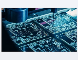
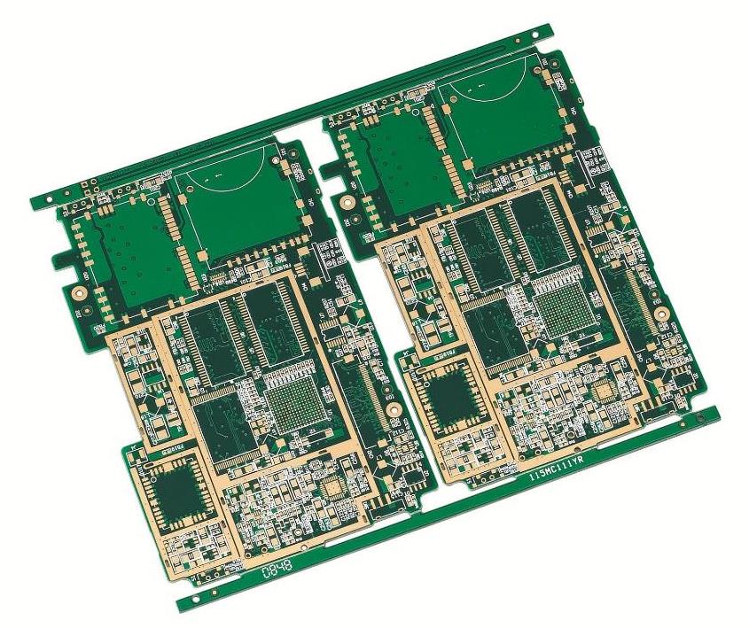
The PCB board is the heart of almost all electronic products, and it carries the components and copper wires that realize its functions. The manufacturing process usually includes electroplating, and the electroplating of different designs will be different. This requires simulation and optimization engineers to constantly create new models. If you can delegate most of the work to the design, engineering and technical personnel who design and manufacture PCB boards, let them do the electroplating simulation by themselves, then what will happen? Come here to see how to achieve it.
1. Customized electroplating simulation software application
You can use the App Developer and the electroplating module in COMSOL Multiphysics version 5.0 to customize the electroplating App. With it, PCB board designers can use simulation to analyze many factors in the design and manufacturing process. They can judge whether a design can meet copper wire specifications, evaluate the performance of such devices, and estimate the manufacturing cost of the electroplating process without having knowledge of electroplating.
2. Design challenges in electroplated copper graphics

Common PCB boards use one or more layers of copper wires to connect the active and passive components on the board. On the other hand, more advanced PCB boards use electroplated copper patterns to generate circuits. Before actually starting electroplating, a layer of patterned insulating film should be prepared on the PCB. This process is achieved through the following steps.
Prepare a layer of patterned insulating film on the PCB board:
The first step is to plate a thin conductive copper seed layer on the PCB. Next, the surface of the PCB board needs to be coated with a layer of photoresist (photosensitive polymer film). This process is usually called photolithography. In this process, the photoresist covering the patterned mask is placed under ultraviolet light, and the exposed area is dissolved. The result is a PCB board with a patterned insulating film and the seed layer at the bottom of the pattern has been exposed.
In the PCB electroplating process, the PCB board and the copper anode (such as a solid copper strip) are immersed in the electroplating tank, which contains an electrolyte of sulfuric acid and copper sulfate. A voltage is applied between the anode and the cathode of the seed layer, which causes an electrochemical reduction reaction, and copper ions are reduced to the copper metal plated (deposited) on the seed layer. As time goes by, the thickness of the coating is directly proportional to the rate of the electrochemical reaction, and the rate is determined by the current density at different positions of the seed layer. Therefore, the patterned photoresist cavity is filled with solid copper. The average current density can be controlled to maintain the plating speed (for example, the total current in the patterned area to be plated).
Finally, the remaining photoresist is removed, and a thin seed layer is etched to separate the different copper-plated wires.
3. Uniformity of electroplating speed:
A known problem in this process is that the plating speed in the entire PCB board is not always uniform. The electric field in the electrolyte is concentrated on the conductive pattern surrounded by the large insulating area and the pattern near the edge of the PCB board. The non-uniformity of the electric field produces a higher local current density on the cathode surface in these regions, and this effect is commonly referred to as current clustering. Over time, the thickness of the plating layer is directly proportional to the current density, which will cause undesirable changes in the thickness of the copper wire in the PCB. This means that the resistance between the copper wires at different positions on the PCB will vary. When PCB boards are used in electronic devices, this thickness variation may be a performance problem, and even in the worst case, the root cause of device failure.
Fourth, the simulation and optimization of the PCB design stage
In order to avoid performance degradation or device failure during the operation of electronic devices, copper wire circuits must meet a set of thickness uniformity specifications. Normally, designers of printed circuit boards rely on simple design rules, such as maximum and minimum line widths, spacing, and pattern density. However, through electroplating simulation, the expected change in copper layer thickness can be calculated more accurately. With this information, the design can be modified at an early stage without waiting for the results of the prototype.
In order to avoid the clustering effect near the edge of the PCB board, a hole with an opening can be placed between the anode and the electroplating tank, that is, an insulating shielding layer. The figure on the right shows the size of the pore opening that can achieve the smallest thickness change after optimization by simulation, and its placement in the electroplating bath.
Fifth, consideration of PCB board manufacturing cost
If PCB board manufacturers want to be competitive, they must consider manufacturing costs. As mentioned earlier, the final product always needs to meet a copper thickness uniformity specification. The thickness uniformity essentially depends on the total plating speed during the electroplating process; the higher the overall speed, the greater the thickness variation. In addition, the total processing time determines the production volume of the production line, and therefore, also determines the manufacturing cost.
Sixth, PCB manufacturing and electroplating costs are minimized
In order to minimize manufacturing costs, processing will be performed at the maximum possible speed that can meet the thickness specifications. By using simulation to study the effect of plating speed, the plating speed that should be used for a given thickness uniformity specification can be calculated. This allows us to estimate the manufacturing cost at the design stage.
By improving the design, or using pores to improve uniformity, the highest electroplating speed that can be supported can be simulated, as well as the cost savings that can be saved in the production of PCB boards.
Seven, run the simulation through the electroplating App
Those who have an electrochemical background and understand simulation models and software created electroplating simulation models. PCB board designers are usually good at electrical design, but have little or no knowledge of electrochemical processes in manufacturing.