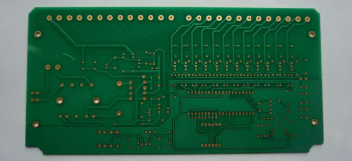
High-frequency board selection of PCB board and production and processing methods
In recent years, wireless communication, optical fiber communication, and high-speed data network products have been continuously launched, information processing has been increased, and wireless analog front-end modularization has put forward new requirements for digital signal processing technology, IC technology, and microwave PCB design. PCB technology puts forward higher requirements.
For example, commercial wireless communication requires the use of low-cost plates, stable dielectric constant (variation error of εr within ±1-2%), and low dielectric loss (less than 0.005). Specific to the PCB board of the mobile phone, it also needs to have the characteristics of multi-layer lamination, simple PCB processing technology, high reliability of the finished board, small size, high integration, and low cost. In order to challenge the increasingly fierce market competition, electronic engineers must compromise between material performance, cost, difficulty in processing technology and the reliability of the finished board. Below, the editor of the circuit board manufacturer will explain in detail how to choose the PCB high-frequency board and its production and processing methods.
1. Definition of high frequency board
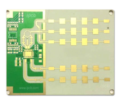
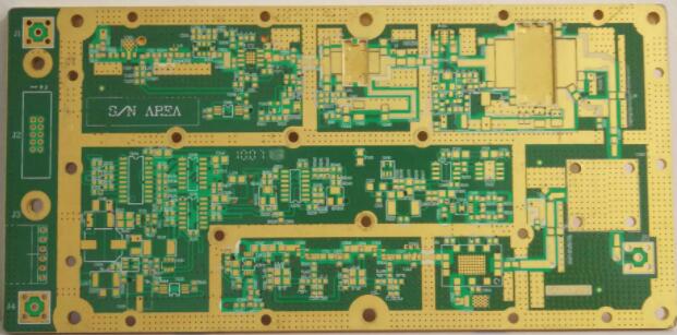
High frequency board refers to the special PCB circuit board with higher electromagnetic frequency, which is used for high frequency (frequency greater than 300MHZ or wavelength less than 1 meter) and microwave (frequency greater than 3GHZ or wavelength less than 0.1 meter). It is a microwave substrate The copper clad board is a circuit board produced by using part of the process of the ordinary rigid circuit board manufacturing method or using a special processing method. Generally speaking, a high-frequency board can be defined as a circuit board with a frequency above 1GHz.
With the rapid development of science and technology, more and more equipment is designed for applications in the microwave frequency band (>1GHZ) or even in the millimeter wave field (30GHZ). This also means that the frequency is getting higher and higher, and the circuit board is The requirements for materials are getting higher and higher. For example, the circuit board substrate material needs to have excellent electrical properties, good chemical stability, and the loss on the substrate with the increase of the power signal frequency is very small, so the importance of the high-frequency board is highlighted.

Two, PCB high-frequency board application field
⑴, mobile communication products;
⑵, power amplifier, low noise amplifier, etc.;
⑶, passive components such as power splitter, coupler, duplexer, filter, etc.;
⑷, automotive anti-collision systems, satellite systems, radio systems and other fields. The high frequency of electronic equipment is a development trend.
Third, the classification of high-frequency boards
⑴, Powder ceramic filled thermosetting material
A. Manufacturer:
4350B/4003C from Rogers;
Arlon's 25N/25FR;
Taconic's TLG series.
B. Processing method:
The processing process is similar to epoxy resin/glass woven cloth (FR4), except that the sheet is relatively brittle and easy to break. When drilling and gongs, the life of the drill nozzle and gong knife is reduced by 20%.
⑵, PTFE (polytetrafluoroethylene) material
A: Manufacturer
1. Taixing Microwave's F4B, F4BM, F4BK, TP-2;
2. Taconic's RF series, TLX series, TLY series;
3.Rogers' RO3000 series, RT series, TMM series;
4. Arlon's AD/AR series, IsoClad series, and CuClad series.
B: Processing method
1. Cutting: the protective film must be kept to prevent scratches and creasing
2. Drilling:
1. Use a brand new drill (standard 130), one by one is the best, the pressure of the presser foot is 40psi;
2. Blow out the dust in the hole with an air gun after drilling;
3. The aluminum sheet is used as the cover plate, and then 1mm melamine backing plate is used to tighten the PTFE plate;
4. Use the most stable drilling rig and drilling parameters (basically, the smaller the hole, the faster the drilling speed, the smaller the Chip load, the lower the return speed).
3. Hole treatment
Plasma treatment or sodium naphthalene activation treatment is conducive to hole metallization.
4.PTH copper sink
1. After the micro-etching (the micro-etching rate has been controlled by 20 microinches), pull the plate into the plate from the de-oil tank in the PTH;
2. If necessary, go through the second PTH, just start the board from the expected cylinder.
5. Solder mask
1. Pre-treatment: use acidic plate washing, mechanical grinding plate is not allowed;
2. After the pre-treatment, the baking board (90 degree Celsius, 30min), brush the green oil to cure;
3. Three-stage baking: one section is 80 degree Celsius, 100 degree Celsius, 150 degree Celsius, and the time is 30min each (if you find that the substrate surface is oily, you can rework: wash off the green oil and reactivate it).
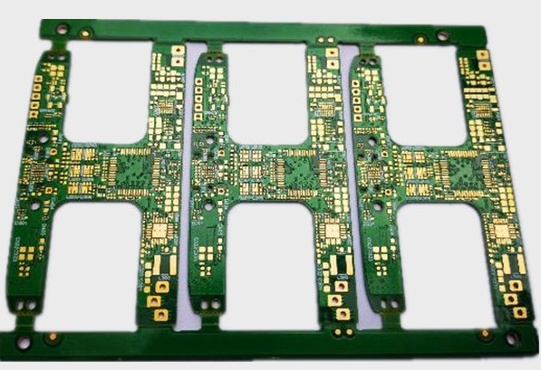
6.Gong board
Lay the white paper on the circuit surface of the PTFE board, and clamp it up and down with the FR-4 base plate or phenolic base plate with a thickness of 1.0MM etched to remove copper: as shown in the figure:
The burrs on the back of the gong board need to be carefully trimmed by hand to prevent damage to the substrate and copper surface, and then separated by a considerable size of sulfur-free paper, and visually inspected. To reduce burrs, the key point is that the effect of the gong board process should be good.
Fourth, the process
1. NPTH's PTFE plate processing flow
Cutting-Drilling-Dry Film-Inspection-Etching-Erosion Inspection-Solder Mask-Characters-Spray Tin-Forming-Testing-Final Inspection-Packaging-Shipment
2. PTH's PTFE plate processing flow
Cutting-drilling-hole treatment (plasma treatment or sodium naphthalene activation treatment)-copper-immersion-plate electricity-dry film-inspection-picture electricity-etching-corrosion inspection-solder mask-character-spray tin-forming-test-final Inspection-Packaging-Shipping
Five: Summary: Difficulties in high-frequency board processing
1. Immersion copper: the hole wall is not easy to be copper;
2. Control of line gaps and sand holes in map transfer, etching, line width;
3. Green oil process: Green oil adhesion and green oil foaming control;
4. Strictly controlled board surface scratches in each process, etc.