How to design challenging high-speed HDI circuit boards
With the increasing requirements for the volume of electronic products, especially the size of mobile device products are developing in the direction of continuous shrinking. For example, the current popular Ultra Book products, and even novel wearable smart devices, must use HDI circuit board height. The carrier board made by density interconnection technology further reduces the size of the terminal design.
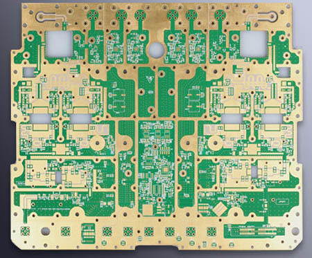
HDI circuit board is a high-density interconnection technology, which is one of the technologies used by printed circuit boards. HDI is mainly produced by the technology of micro-blind and buried vias. Its characteristic is to make the electronic circuit distribution in the printed circuit board higher. However, due to the large increase in circuit density, the printed circuit board made of HDI cannot be used for general drilling. Hole formation, HDI must use a non-mechanical drilling process. There are many non-mechanical drilling methods. Among them, "laser hole formation" is the main hole formation solution of HDI high-density interconnection technology.

HDI printed circuit boards have a wide range of applications. For example, mobile phones, ultra-thin laptops, tablet computers, digital cameras, automotive electronics, digital cameras... and other electronic products have used HDI technology to reduce the motherboard design and reduce the benefits. Quite large, not only the design of the terminal product can leave more space in the organization for batteries or more additional functional components, but the cost of the product can also be relatively reduced due to the introduction of HDI.
HDI was used in mid- and high-priced mobile phones in the early days, and now it is almost universal in all mobile devices.
The products that used the most HDI technology in the early days were mainly functional phones and smart phones. Such products accounted for more than half of the HDI high-density circuit board consumption, while Any-layer HDI (any layer high-density interconnection board) was the highest The biggest difference between the high-level HDI manufacturing process and the general HDI circuit board is that most HDI is machined by a drilling process for PCB penetration processing. As for the plates between layers, Any-layer HDI uses "laser" drilling. Open up the interconnection design of each layer.
For example, the Any-layer HDI production method can generally save about 40% of the PCB volume. At present, Any-layer HDI has been used in Apple iPhone 4, or newer smart phones, with higher-density integrated motherboards. Reduce the thickness of product design, so that product design can be marketed with a thinner and lighter design. However, Any-layer HDI is manufactured using laser blind holes, which are relatively difficult to manufacture and cost more than ordinary circuit boards. At present, mobile devices with only high unit prices are used more.
HDI printed circuit boards are manufactured using the build-up method (Build Up). The technological gap of HDI lies in the number of build-ups. The more circuit layers, the higher the technical difficulty! For general-purpose HDI boards, basically one-time build-up can be used. As for high-end HDI boards, they are manufactured with two or more build-up build-up techniques to avoid mechanical perforation that causes high-density HDI boards. The wiring is damaged due to improper drilling, and the hole forming process can simultaneously use advanced printed circuit board manufacturing techniques such as laser perforation, electroplating hole filling, and stacked holes.
Key components with high pin counts need to use HDI for product design
Especially FPGA components with a large number of pins are a great trouble for PCB wiring. Another example is the most common GPU components at present. The number of pins is also developing more and more. Most of them have been switched to HDI printed circuit boards. For product design, HDI boards are especially suitable for design schemes that require highly complex connections.
Especially for the new generation of SoC or integrated chips, its highly integrated functions have led to more and more IC pins, which greatly increases the difficulty of PCB design connection lines, and HDI high-density circuit board design solutions can use multiple layers inside the board. The advantage of interconnection and integration is to complete the connection of complex chip pins one by one, and the laser blind hole production can make micro blind holes in the plate, which can be perforated, staggered, stacked, or on any layer. For interconnection, the layout flexibility of the circuit is relatively higher than that of the traditional PCB, and it also provides an easier board design solution for the integrated chip application solution with high pin count.
The HDI circuit board design is also more complicated than the previous PCB circuit boards. Not only does the circuit become tighter, the design complexity of using different layers of circuit interconnection is also greatly improved, and the circuit becomes thinner and tighter, but also It means that the conductor cross-sectional area of the circuit has been changed small, which will cause the integrity of the transmitted signal to be more prominent, and it is necessary for PCB design engineers to spend more time on verifying and troubleshooting the board function.
Especially in the face of highly complex design cases, such as the possibility of design changes in the electronic circuit of the board during the development process is quite high, and if the core components of the motherboard are FPGAs or other components with a large number of pins, a slight design change is required. It will cause delays in the design improvement timeline. How to minimize circuit deployment errors in the process of frequent design changes must be equipped with design aids that can support HDI high-complexity circuit design, especially with FPGA logic Under the design framework where design, hardware design, PCB logic and related design data are interoperable, any project design specification changes can be reflected in the development system in real time, avoiding design problems that cannot match the design board and the target chip.
HDI requires high-density lines, and lasers are needed to make holes
In fact, there is no clear definition of HDI high-density manufacturing method, but in general, the difference between HDI and non-HDI is quite large. First of all, the hole diameter of the circuit carrier made of HDI must be less than or equal to 6mil (1/1,000 inch). As for the ring diameter of the aperture ring, it needs to be ≦10mil, and the layout density of the line contacts needs to be greater than 130 points per square inch, and the line spacing of the signal lines needs to be 3mil or less.
HDI printed circuit boards have many advantages. HDI has a high degree of integration of circuits, so the area of the board can be greatly reduced, and the higher the number of layers, the shrinkable board surface can also increase correspondingly. Due to the smaller size of the substrate, HDI applications The surface area of the circuit board can be 2 to 3 times smaller than the non-HDI circuit board design, but it can maintain the same complex circuit, and the material weight of the natural board can be reduced by this. As for the circuit design of specific blocks such as radio frequency and high frequency, multi-layer structure can be made good use of. A large area of metal grounding layer is set on the upper/lower circuit of the main circuit to limit the EMI problems of high-frequency circuits that may be caused by the PCB. The inside of HDI board avoids affecting the operation of other external electronic equipment.
The HDI board is lighter in weight and higher in line density, and the space utilization rate in the chassis is relatively higher than that of the non-HDI circuit board design. The original high-frequency operating device will increase the transmission distance of the signal line due to the use of HDI. Shortened, naturally beneficial to the signal transmission quality of new SoC or high-frequency operating devices. Because of the better electrical characteristics, the transmission efficiency is improved. In addition, if the HDI uses more than 8 layers, you can basically get better than non-HDI circuit boards. Cost-effective. For terminal product design, HDI motherboard design solutions can also be used to improve product performance and specification data performance, making products more competitive in the market.
HDI circuit board design requires more careful product verification
It is also because the HDI printed circuit board has greatly increased the circuit complexity, which will bring more design load to the original PCB layout design work. In the actual development project, although the auxiliary development software can be used for rapid wiring Deployment and positioning, but in fact, it is still necessary to match the design experience of the developer to optimize the component configuration and circuit layout. With the development software, it will automatically correspond to the connection between the pins and the circuit, and the relative position will automatically change the circuit pins. And other automated design solutions to further simplify the HDI printed circuit board design process and reduce the lengthy development schedule.
In addition, HDI is often also used in the design and application of high-speed components, especially now that 3C or mobile devices have a GHz-level operating clock at all times, the direction of the motherboard circuit will also affect the equipment under high-frequency operation. Impact of EMI/EMC issues. Generally speaking, you can first use the development software to set the design parameters of timing rules and routing topology, provide the development software with a reference range of constraints, and then use the software verification function of the development software to carry out the preliminary design. Machine verification, of course, the native circuit verification of the development software is not a real circuit debugging after all. At most, it can only be used as a reference for development. The actual design plan must be verified for many times before making a reference design for HDI board function verification.
There are many benefits to using software simulation verification. Basically, software simulation verification can be used to quickly find out the logic circuit that may be wrong, check points and lines through the design software, and check the blocks that may have wrong design, and the software simulation The speed is quite fast. It can be used as the basis for verification before small batch production of plates. After software verification and simulation environment testing have no problems, the trial products can be physically verified, which can greatly reduce HDI development costs.