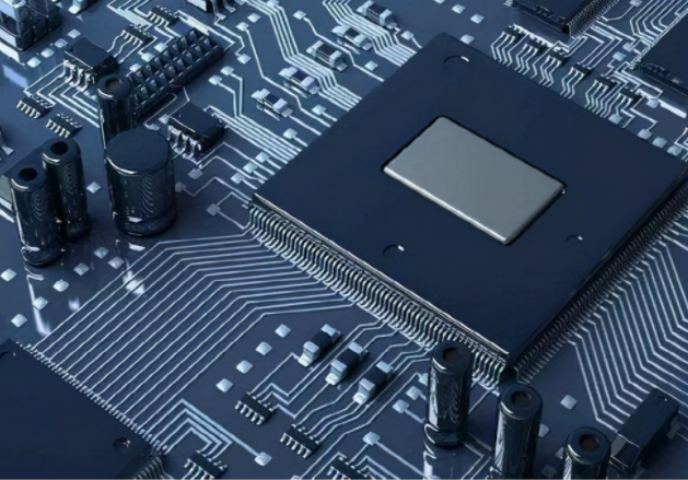
What are the feasible processes for PCB proofing production
1. Line
1. Minimum line width: 6mil (0.153mm). That is to say, if the line width is less than 6mil, it will not be able to produce (the minimum line width and line spacing of the inner layer of the multilayer circuit board is 8MIL) If the design conditions permit, the larger the design, the better, the line width rises, the better the PCB proofing factory produces, good The higher the rate, the general design convention is about 10mil, this point is very important, the design must be considered.
2. Minimum line spacing: 6mil (0.153mm). The minimum line distance is line-to-line, and the distance from line to pad is not less than 6mil. From a production point of view, the larger the better, the general rule is 10mil. Of course, the larger the better, the design is very important. Design Must be considered.
3. The distance between the line and the outline line is 0.508mm (20mil).

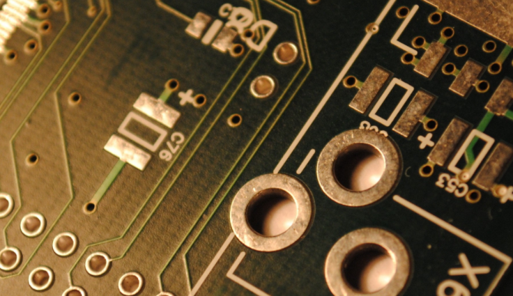
Second, via vias (commonly known as conductive holes)
1. Minimum aperture: 0.3mm (12mil).
2. The distance between the pad and the outline line is 0.508mm (20mil).
3. Via hole (VIA) hole-to-hole spacing (hole edge to hole edge) cannot be less than 6mil, preferably greater than 8mil. This point is very important, and the design must be considered.
4. The minimum via hole (VIA) aperture is not less than 0.3mm (12mil), and the single side of the pad cannot be less than 6mil (0.153mm), preferably greater than 8mil (0.2mm), but not limited. This point is very important, and the design must be consider.
3. PAD pad (commonly known as plug-in hole (PTH))
1. The distance between the pad and the outline line is 0.508mm (20mil).
2. Plug-in hole (PTH) The outer ring of the pad should not be less than 0.2mm (8mil) on one side. Of course, the larger the better, this point is very important, and the design must be considered.
3. Plug-in hole (PTH) hole-to-hole spacing (hole edge to hole edge) cannot be less than 0.3mm. Of course, the bigger the better, this is very important, and the design must be considered.
4. The size of the plug-in hole depends on your component, but it must be larger than the pin of your component, and it is recommended to be larger than at least 0.2mm. That is to say, for the component pins of 0.6, you have to design at least 0.8 to prevent difficult insertion due to machining tolerances.
4. Solder proof: open the window for the plug-in hole, and the single side of the SMD window cannot be less than 0.1mm (4mil).
5. Characters (the design of the characters directly affects the production. Whether the characters are clear or not depends on the character design). The character width cannot be less than 0.153mm (6mil), the character height cannot be less than 0.811mm (32mil), and the width ratio The height ratio is preferably a relationship of 5. In other words, the character width is 0.2mm and the character height is 1mm, and so on.
6. Non-metalized slots: The minimum spacing of slots is not less than 1.6mm, otherwise it will greatly increase the difficulty of milling.
Seven, imposition
1. V-cutting can only go in a straight line. Due to the shape of the board, the distance can be added for the stamp hole bridge connection and related precautions.
2. The size of the imposition V-cut direction must be greater than 8cm, because V-cuts smaller than 8cm will fall into the machine when cutting. The width of the V-cut must be less than 32cm. If the width is greater than this width, it will not fit into the V-cut machine. The production process is limited, not that we can't do it.
3. The imposition is divided into no-gap imposition and gap imposition. The imposition gap with gap imposition should not be less than 1.6 (plate thickness 1.6) mm, otherwise it will greatly increase the difficulty of milling. The size of the imposition work board will vary depending on the equipment. The gap of no-gap imposition is about 0.5mm, and the process edge is generally 5mm.
iPCB is a high-tech manufacturing enterprise focusing on the development and production of high-precision PCBs. iPCB is happy to be your business partner. Our business goal is to become the most professional prototyping PCB manufacturer in the world. Mainly focus on microwave high frequency PCB, high frequency mixed pressure, ultra-high multi-layer IC testing, from 1+ to 6+ HDI, Anylayer HDI, IC Substrate, IC test board, rigid flexible PCB, ordinary multi-layer FR4 PCB, etc. Products are widely used in industry 4.0, communications, industrial control, digital, power, computers, automobiles, medical, aerospace, instrumentation, Internet of Things and other fields.

![[Hot spot] PCB manufacturers say they are not worried about orders, but materials are in short supply](/public/upload/image/20210912/e19e03ee3b747407916c98d1a943eb17.png)