What are the requirements of PCB manufacturing process for pads?
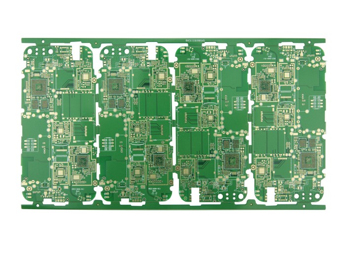
The pad is the basic unit of PCB surface mount assembly. As an excellent PCB engineer, it is essential to have a wealth of knowledge reserves of pads. So, do you know what the PCB manufacturing process requires for pads? Let's learn more about it together:
1. Test points should be added to the pads where the two ends of the chip components are not connected to the plug-in components. The diameter of the test points is equal to or greater than 1.8mm to facilitate the on-line tester test.
2. For IC pin pads with dense pin spacing, if they are not connected to the hand plug-in pads, test pads need to be added. The diameter of the test point is equal to or greater than 1.8mm to facilitate online tester testing.
3. If the distance between the pads is less than 0.4mm, white oil must be applied to reduce continuous soldering when the wave crest is exceeded.
4. The two ends and ends of the SMD component should be designed with lead-tin, and the lead-tin width is recommended to use 0.5mm wire, and the length is generally 2 or 3mm.

5. If there are hand-soldering components on the single panel, remove the tin bath, the direction is opposite to the soldering direction, and the width of the hole is 1.0mm to 0.3mm.
6. The spacing and size of the conductive rubber buttons should be consistent with the actual size of the conductive rubber buttons. The PCB board connected to this should be designed as a gold finger, and the corresponding gold plating thickness should be specified.
7. The size and spacing of the pad should be exactly the same as the size of the patch component.
The above are the requirements of PCB manufacturing process for pads. How much do you know?
iPCB is a high-tech manufacturing enterprise focusing on the development and production of high-precision PCBs. iPCB is happy to be your business partner. Our business goal is to become the most professional prototyping PCB manufacturer in the world. Mainly focus on microwave high frequency PCB, high frequency mixed pressure, ultra-high multi-layer IC testing, from 1+ to 6+ HDI, Anylayer HDI, IC Substrate, IC test board, rigid flexible PCB, ordinary multi-layer FR4 PCB, etc. Products are widely used in industry 4.0, communications, industrial control, digital, power, computers, automobiles, medical, aerospace, instrumentation, Internet of Things and other fields.