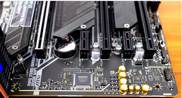
Detailed explanation of the PCB circuit board plugging process for you
The vias play the role of interconnection and conduction of the lines. The development of the electronics industry also promotes the development of PCBs, and also puts forward higher requirements on the production process and surface mount technology of the printed circuit board, and the plugging process has emerged at the historic moment. Now, let the engineer explain the PCB circuit board plugging process for you in detail:
1. Hole plugging process after hot air leveling
Non-plugging process is adopted for production. After hot air leveling, aluminum sheet screen or ink blocking screen is used to complete the via hole plugging of all fortresses. The process flow is: board surface soldering - hot air leveling - plugging - curing.
This process can ensure that the through holes will not lose oil after the hot air is leveled, but it is easy to cause the plugging ink to contaminate the board surface and uneven.
2. Hot air leveling and plug hole technology

1. Use aluminum sheet to plug the hole, solidify, and polish the board to transfer the graphics
In this process, a numerical control drilling machine is used to drill the aluminum sheet that needs to be plugged into a screen, and then plug the holes. The process flow is: pre-treatment - plug hole - grinding plate - pattern transfer - etching - board surface solder mask.
This method can ensure that the via hole plug is flat, and hot air leveling will not cause quality problems such as oil explosion and oil drop on the hole edge. However, this process requires one-time thickening of copper, which requires high copper plating on the entire board.
2. After plugging the hole with aluminum sheet, directly screen-print the surface of the board for solder mask
This process uses a CNC drilling machine to drill out the aluminum sheet that needs to be plugged to make a screen, install it on the screen printing machine for plugging, park it for no more than 30 minutes, and directly screen the surface of the board with a 36T screen. The process flow is: pre-treatment-plug hole-silk screen-pre-baking-exposure-development-curing
This process can ensure that the via hole cover is well oiled, the plug hole is flat, the via hole will not be tinned after hot air leveling, and there will be no tin beads in the hole, but it is easy to cause the ink in the hole to be on the pad after curing, poor solderability, etc. .
3. The aluminum sheet is plugged into the hole, developed, pre-cured, and soldered on the surface after grinding.
Use a CNC drilling machine to drill out the aluminum sheet that requires plugging holes to make a screen, install it on the shift screen printing machine for plugging holes, the plugging holes must be full, and then solidified, and the board is polished for surface treatment. The process flow is: pre-treatment-plug hole-pre-baking-development-pre-curing-board surface solder mask
This process can ensure that the through holes will not drop or explode after the hot air is leveled, but it is difficult to completely solve the problem of tin beads in the through holes and tin on the via holes.
4. The board surface solder mask and plug hole are completed at the same time
This method uses a 36T (43T) screen, which is installed on the screen printing machine, using a backing plate or a bed of nails, and when completing the board surface, all the through holes are plugged. The process flow is: pre-treatment-silk screen-pre-baking-exposure-development-curing.
The process time is short and the utilization rate of the equipment is high. It can ensure that the via holes will not lose oil and the via holes will not be tinned after hot air leveling. However, due to the use of silk screens for plugging, a large amount of air is trapped in the via holes, resulting in voids and unevenness., There are a few via holes hidden tin.
The above is the PCB circuit board plugging process explained by PCB factory engineers in detail. I hope it will be helpful to customers and friends.