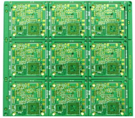
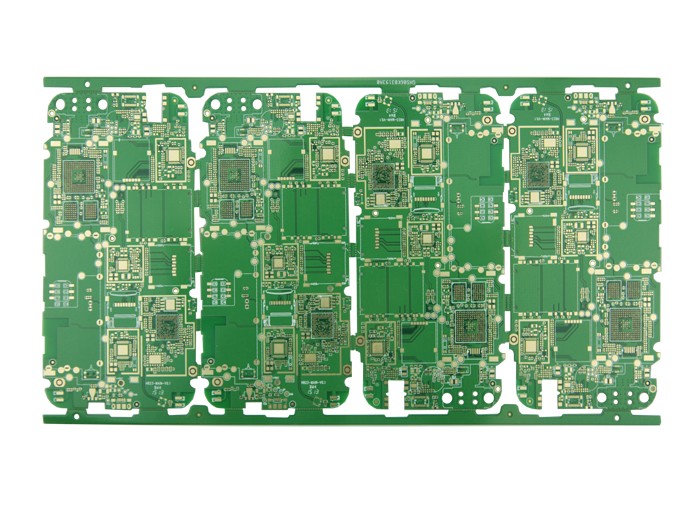
With the improvement of product performance, PCB boards are constantly being updated and developed, circuits are becoming more and more dense, and more and more components need to be placed. However, the size of PCB boards will not become larger, but become smaller and smaller. So, if you want to drill holes in the plate at this time, you need considerable skills. To
There are many PCB board drilling techniques. The traditional method is to make inner blind holes. When laminating the multilayer board successively, first use two double-sided boards with through holes as the outer layer, and press them with the non-porous inner board., The blind holes that have been filled with glue appear, and the blind holes on the outer plate surface are formed by mechanical drilling. However, when making machine-drilled blind holes, it is not easy to set the drilling depth of the drill bit, and the tapered hole bottom affects the effect of copper plating. In addition, the process of making inner blind holes is too long and wastes too much cost. Traditional methods More and more unsuitable. To

Nowadays commonly used PCB board micro-hole technology, in addition to the carbon dioxide drilling and laser drilling we introduced before, there are mechanical drilling, photosensitive drilling, laser drilling, plasma etching and chemical etching. To
Mechanical drilling is made by high-speed machining, the most important of which is the drill bit. The drill bit is generally made of tungsten-cobalt alloy. The alloy uses tungsten carbide powder as the matrix and cobalt as the binder. With high hardness and high wear resistance, the required holes can be drilled smoothly. To
Laser hole formation is made by carbon dioxide and ultraviolet laser cutting. The gas or light forms a beam of light, which has powerful heat energy and can burn through the copper foil to create the required hole. The principle is the same as cutting, mainly to control the beam. To
Plasma is also plasma. The particles that make up the plasma have a large distance between them and are in constant and random collisions. Its thermal motion is similar to that of ordinary gas. Plasma etch holes are mainly used for the PCB board of the resin copper layer. Oxygen-containing gas is used as the plasma. After contact with the copper, an oxidation reaction will occur, and the resin material will be removed to form the hole. To
As mentioned befor
e, the remaining objects on the PCB board can not be cleaned by the general method. You can use chemical cleaning to make the chemical agent react with the residue, and then it can be removed. The same is true for drilling. Use chemical agents and drop them on the place where drilling is needed to erode the copper foil, resin, etc., and finally form holes.
The above is an introduction to the common methods of PCB board drilling technology. Ipcb also provides PCB manufacturers, PCB manufacturing technology, etc.