Common sense of high frequency PCB wiring (5)
PCB factory: 1. How to reduce EMI problems through organization and layering?
First of all, EMI must be considered from the system. PCB alone cannot solve the problem. As far as EMI is concerned, lamination is mainly to provide the shortest return path for the signal, reduce the coupling area, and suppress differential mode interference. The other stratum is tightly coupled with the power layer, which is properly extended than the power layer, and has advantages in suppressing common mode interference.
2. Why should copper be laid?
There are generally several reasons for copper paving. 1. EMC. For large-area ground or power supply copper, it will play a shielding effect, and some special grounds, such as PGND, play a protective effect. 2. PCB process requirements. Generally, in order to ensure the effect of electroplating, perhaps the laminate is not deformed, and copper is laid on the PCB layer with less wiring. 3. The signal integrity is required to give high-frequency digital signals a sound
Return paths and reduce the wiring of the DC network. Of course, there are also reasons for heat dissipation, special equipment and installations requiring copper to be laid.
")
3. In a system, dsp and pld are included. What problems should be paid attention to when wiring?
Look at the ratio of your signal rate to the length of the wiring. If the time delay of the signal in the transmission line is comparable to the signal change edge time, the signal integrity problem must be considered. Other issues related to multiple DSPs, clocks, and data signal routing will also affect signal quality and timing, which requires attention.
4. In addition to the protel wiring, are there other good things?
As for things, in addition to PROTEL, there are many wiring tools, such as MENTOR's WG2000, EN2000 series and powerpcb, Cadence's allegro, Zuken's cadstar, cr5000, etc., each with its own strengths.
5. What is the "signal return path"?
The signal return path is return current. When high-speed digital signals are being transmitted, the signal flows from the driver along the PCB transmission line to the load, and then from the load back to the driver through the shortest path along the ground or power supply. This return signal on the ground or power supply is called the signal return path. Dr. Johson explained in his book that high-frequency signal transmission is actually
The process of charging the dielectric capacitor sandwiched between the transmission line and the DC layer. SI analyzes the electromagnetic characteristics of the enclosure and the coupling between them.
6. How to perform SI analysis on connectors?
In the IBIS3.2 standard, there is a description of the connector model. The EBD model is generally used. If it is a special board, such as a backplane, a SPICE model is required. It is also possible to use multi-board simulation software (HYPERLYNX or IS_multiboard) to input the distribution parameters of the connectors when establishing a multi-board system, which is generally obtained from the connector manual. Of course this method will not be precise
Yes, but as long as it is within the acceptable range.
7. What are the termination methods?
Termination (terminal), also known as matching. Generally, it is divided into active end matching and terminal matching according to the matching orientation. The source terminal matching is generally resistance series matching, and the terminal matching is generally parallel matching. There are many methods, including resistance pull-up, resistance pull-down, Thevenin matching, AC matching, and Schottky diode matching.
8. What factors determine the choice of termination (matching) method?
The matching selection method is generally determined by the BUFFER characteristics, topological status, level variety and judgment method, and the signal duty cycle, system power consumption, etc. should also be considered.
9. What are the rules for choosing the termination (matching) method?
The most critical aspect of digital circuits is the timing issue. The purpose of adding matching is to improve the signal quality and obtain a determinable signal at the decision time. Regarding level useful signals, the signal quality is stable under the premise of ensuring the establishment and persistence of time; for useful signals, under the premise of ensuring the monotonicity of signal delay, the signal change delay speed meets the requirements.
10. Can the IBIS model of the equipment be used to simulate the logical function of the equipment? If not, how to perform board-level and system-level simulation of the circuit?
The IBIS model is a behavioral model and cannot be used for functional simulation. For functional simulation, SPICE model or other structural model may be used.
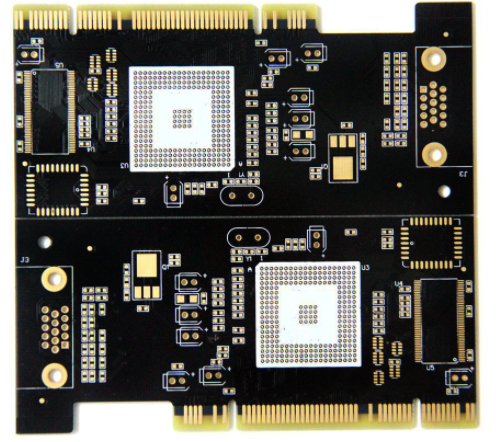
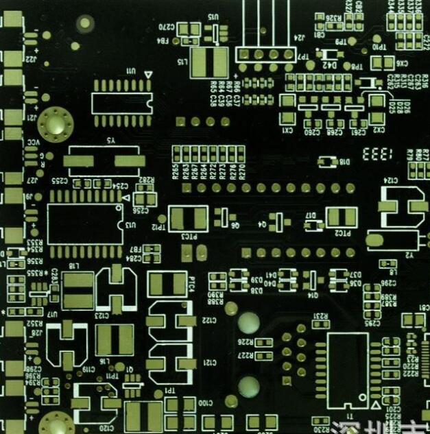
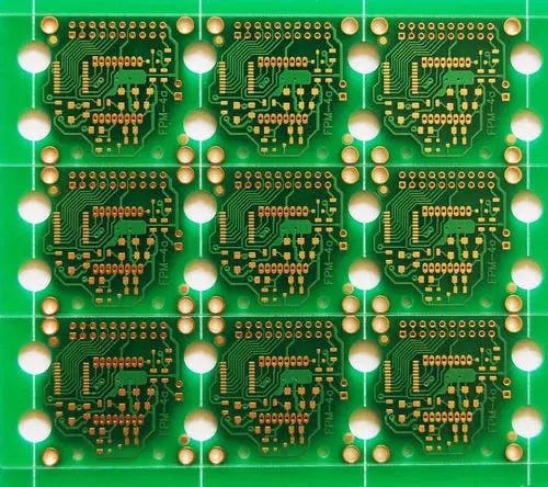
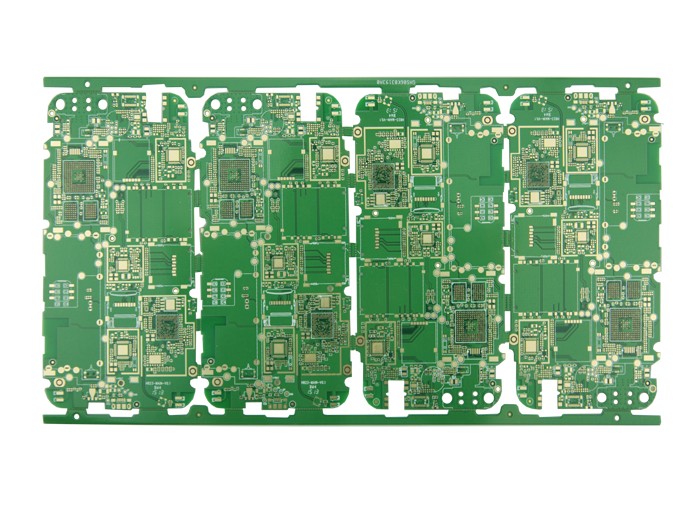
ipcb is a high-precision, high-quality PCB manufacturer, such as: isola 370hr PCB, high-frequency PCB, high-speed PCB, ic substrate, ic test board, impedance PCB, HDI PCB, Rigid-Flex PCB, buried blind PCB, advanced PCB, microwave PCB, telfon PCB and other ipcb are good at PCB manufacturing.