Common sense of high frequency PCB wiring (3)
1. How to choose EDA stuff
In the current PCB board planning software, thermal analysis is not a strong point, so it is not recommended to use it. Other functions 1.3.4 can choose PADS or Cadence. The performance and price ratio are good. Beginners in PLD planning can choose the integrated environment provided by PLD chip manufacturers, and can choose single-point items when planning more than one million gates.
2. Please recommend an EDA software suitable for high-speed signal processing and transmission.
Conventional circuit planning, INNOVEDA's PADS is very good, and there is a matching simulation software, and this type of planning often occupies 70% of the use occasions. When doing high-speed circuit board planning, imitation and digital hybrid circuits, Cadence’s solution should be attributed to software with better performance and price. Of course, Mentor’s performance is still very good, especially it
The planning process should be the best.
")
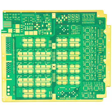
3. Explanation of the meaning of each layer of the PCB board
Topoverlay ---- The title of top equipment, also called top silkscreen or top component legend, such as R1 C5,
IC10.bottomoverlay----similarly to multilayer-----if you plan a 4-layer board, and you place a free pad or via, define it as a multilayer, then its pad will automatically appear on the 4 layers. If you only define it as a top layer, then its pad will only appear on the top layer.
4. High-frequency PCB planning, routing, layout, and layout above 2G, which aspects should be paid attention to
High-frequency PCBs above 2G belong to RF circuit planning and are not within the scope of comments on high-speed digital circuit planning. The layout and routing of the radio frequency circuit should be considered together with the schematic, because the layout and routing will all have a spreading effect. In addition, some passive devices in the radio frequency circuit planning are parameterized and defined, and the special-shaped copper foil is completed, so it is required
EDA tools can provide parameterized equipment, and can modify special-shaped copper foils. Mentor's boardstation has a dedicated RF planning module that can meet these requirements. Moreover, general radio frequency planning requires special radio frequency circuit analysis tools. The most famous in the industry is Agilent's eesoft, which has a good interface with Mentor's tools.
5. For high frequency PCB planning above 2G, what rules should be followed for microstrip planning?
RF microstrip line planning requires three-dimensional field analysis to extract transmission line parameters. All rules should be ruled out in this field.
6. Regarding the all-digital signal PCB, there is an 80MHz clock source on the board. In addition to the selection of wire mesh (grounding), in order to ensure satisfactory driving ability, what kind of circuit should be used for maintenance?
To ensure the driving ability of the clock, it should not be completed after maintenance. Generally, a clock driving chip is used. The general concern about clock driving ability is due to the formation of multiple clock loads. Choose clock drive chip, change one clock signal into several, choose point-to-point connection. Select the driver chip, in addition to ensuring that the load is fundamentally matched, the signal edge meets the requirements (generally, the clock is
Effective signal), when calculating the system timing, the time delay of the clock in the drive chip should be counted.
7. If a separate clock signal board is used, what kind of interface is generally used to ensure that the transmission of the clock signal is less affected?
The shorter the clock signal, the smaller the transmission line effect. Choosing a separate clock signal board will add signal wiring length. And the grounding power supply of the single board is also a problem. If long-distance transmission is required, differential signals are recommended. The LVDS signal can satisfy the driving requirements, but your clock is not too fast, it is not necessary.
8. 27M, SDRAM clock lines (80M-90M). The second and third harmonics of these clock lines are just in the VHF band, and the interference will be great after the high frequency enters from the receiving end. In addition to shortening the line length, what other good methods are there?
If the third harmonic is large and the second harmonic is small, it may be because the signal duty cycle is 50%. In this case, the signal has no even harmonics. At this time, the signal duty cycle needs to be corrected. In addition, if it is a unidirectional clock signal, the source terminal is generally selected for series matching. This can suppress the secondary reflection, but will not affect the clock edge rate. Source matching value, can be selected
The formula in the figure below is obtained.
9. What is the topology of the wiring?
Topology, and some are also called routing order. The routing order of the multi-port connection network.
10. How to adjust the routing topology to improve signal integrity?
The direction of this kind of network signal is more complicated. Because of the different topological effects on unidirectional, bidirectional signals, and signals of different levels, it is difficult to say which topology is beneficial to signal quality. And when doing the pre-simulation, which topology to choose is very demanding for the engineer, and it is required to understand the circuit principle, signal type, and even the difficulty of wiring.
ipcb is a high-precision, high-quality PCB manufacturer, such as: isola 370hr PCB, high-frequency PCB, high-speed PCB, ic substrate, ic test board, impedance PCB, HDI PCB, Rigid-Flex PCB, buried blind PCB, advanced PCB, microwave PCB, telfon PCB and other ipcb are good at PCB manufacturing.