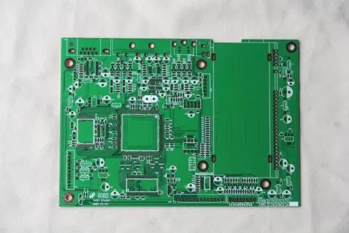
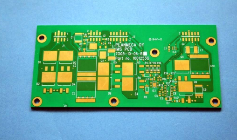
Electromagnetic compatibility (EMC) and associated electromagnetic interference (EMI) have always required the eyes of system design engineers, especially PCB layout and design engineers, as printed circuit board design and component packages shrink and Oems demand ever faster systems.
EMC is closely related to the generation, propagation and reception of electromagnetic energy, and is not desirable in PCB design. Electromagnetic energy comes from multiple sources and is mixed together, so special care must be taken to ensure that signals are compatible and do not interfere with each other when different circuits, wiring, perforations and PCB materials work together.

EMI, on the other hand, is a destructive effect caused by EMC or unwanted electromagnetic energy. In this electromagnetic environment, PCB designers must ensure that electromagnetic energy generation is reduced to make interference.
Here are 7 tips to avoid electromagnetic problems in PCB design:
Tip 1: Ground the PCB
An important way to reduce EMI is to design PCB grounding. The step is to make the grounding area within the total area of the PCB board as large as possible, which can reduce emission, crosstalk and noise. Care must be taken when connecting each component to the ground or ground layer, otherwise the reliable neutralization of the ground layer cannot be fully utilized.
A particularly complex PCB design has several stable voltages. Ideally, each reference voltage has its own grounding layer. However, if there are too many ground layers, it will increase the manufacturing cost of PCB and make the price too high. The compromise is to use grounding layers at three to five different locations, each of which may contain multiple grounding sections. This not only controls the manufacturing cost of the circuit board, but also reduces EMI and EMC.
Low impedance grounding systems are important if EMC is to be implemented. On multilayer PCBS, there is a reliable thieving layer instead of a copper counterbalance or scattered thieving layer as it has low impedance and can provide current paths that are the reverse signal source.
To address EMC issues in multilayer PCBS, there is a solid thieving layer instead of copper counterbalance or scattered thieving layers.
The time it takes for the signal to return to earth is also important. The time between the signal and the source must be equal; otherwise, an antenna - like phenomenon will occur and the radiated energy will become part of the EMI. Similarly, the route of the current to/from the signal source should be as short as possible. If the length of the source path and the return path is not equal, there will be a grounding bounce, which will also generate EMI.
If the time of the signal in and out of the signal source is not synchronized, an antenna like phenomenon will occur, which radiates energy and causes EMI.
Tip 2: Distinguish EMI
Because of the EMI differences, a good EMC design rule is to separate analog and digital circuits. Analog circuits with high amperes or high current should be kept away from high-speed wiring or switching signals. If possible, they should be protected by ground signals. On multi-layer PCBS, analog wiring should be on one grounding and switch wiring or hig
h-speed wiring should be on another grounding. As a result, signals of different properties are separated.
High-frequency noise coupled to surrounding routing can sometimes be eliminated with a low-pass filter. Filters can suppress noise and return a steady current. It is important to separate the grounding of analog and digital signals. Because analog and digital circuits have unique characteristics, it is important to separate them. Digital signals shall have digital grounding and analog signals shall terminate at analog grounding.
In digital circuit design, experienced PCB layout and design engineers pay special attention to high-speed signals and clocks. At high speeds, the signal and clock should be as short as possible and close to the ground, which, as mentioned earlier, keeps crosstalk, noise and radiation within manageable limits.
Digital signals should also be kept away from the power plane. If it is too close, it can produce noise or induction, which can weaken the signal.
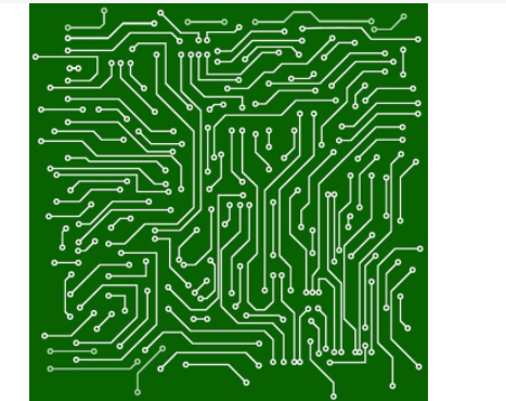
Tip 3: Crosstalk and wiring are the focus
Wiring is especially important to ensure the normal flow of current. If the current is coming from an oscillator or other similar device, it is especially important to keep the current separate from the grounding or not to have the current in parallel with another line. Two parallel high-speed signals can produce EMC and EMI, especially crosstalk. The resistance path must be short and the return current path as short as possible. The length of the return route must be the same as that of the send route.
For EMI, one is called "intrusion wiring" and the other is "victimization wiring". Inductance and capacitance coupling can affect the "victim" wiring due to the presence of electromagnetic fields, thus generating forward and reverse currents on the "victim wiring". In this way, the ripple is produced in a stable environment where the length of the signal sent and received is almost equal.
In a well-balanced and stable wiring environment, the induced currents should cancel each other out to eliminate crosstalk. But we live in an imperfect world, and that doesn't happen. Therefore, the goal must be to keep all crosstalk in line at a level. If the width between parallel lines is twice the width of the lines, the effect of crosstalk can be reduced to. For example, if the line width is 5 mils, the distance between two parallel lines should be 10 mils or more.
PCB designers must also continue to grapple with emc and interference issues as new materials and components emerge.
Tip 4: Decoupling capacitors
Decoupling capacitors reduce the adverse effects of crosstalk. They should be located between the power and ground pins of the device to ensure a low AC impedance and reduce noise and crosstalk. To achieve low impedance over a wide frequency range, multiple decoupling capacitors should be used.
Crosstalk can be reduced by using a decoupling capacitor around a spherical grid array. (Image: NexLogic) An important principle for placing decoupling capacitors is to place capacitors with capacitance values as close to the device as possible to reduce inductive impact on wiring. This particular capacitor is placed as close as possible to the power pin or power cable of the equipment and the pad of the capacitor is connected directly to the through hole or ground. If the cable is long, use multiple through-holes to ensure grounding impedance.
Tip 5: Avoid 90° angles
To reduce EMI, avoid 90° angles formed by wiring, perforations, and other components, because the right Angle will generate radiation. At this Angle the capacitance will increase and the characteristic impedance will change, leading to reflection and thus EMI. To avoid 90° angles, wiring should be routed at least two 45° angles to corners.
Tip 6: Use holes with caution
In almost all PCB layouts, perforations must be used to provide a conductive connection between the different layers. PCB layout engineers need to be especially careful because of the inductance and capacitance generated through the holes. In some cases, they also reflect because the characteristic impedance changes as holes are made in the wiring.
Also keep in mind that perforations increase the length of the line and need to be matched. If differential wiring is used, through holes should be avoided as far as possible. If this cannot be avoided, through-holes should be used in both routes to compensate for delays in the signal and return paths.
Tip 7: Cable and physical shielding
Cables carrying digital circuits and analog currents can generate parasitic capacitors and inductors, causing many EMC-related problems. If twisted pair cables are used, the coupling level is kept low, eliminating the resulting magnetic field. For high frequency signals, shielded cables must be grounded on both the front and back to eliminate EMI interference.
Physical shielding is a metal package that covers the whole or part of the system and prevents EMI from entering the PCB circuit. This shielding acts as a closed grounding conductive container, reducing the size of the antenna loop and absorbing EMI.