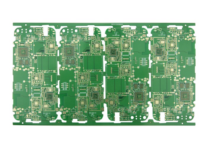
The key to the success or failure of any technical job is some details, especially for the PCB board industry. In the circuit board design, what key details should be paid attention to in order to ensure that the circuit board design is worry-free?

1. Standard components should pay attention to the component size tolerances of different manufacturers. Non-standard components must be designed according to the actual size of the component and the pad pattern and pad spacing.
2. When designing a highly reliable circuit, the pad should be widened (pad width = 1.1 component width).
3. When the density is high, the pad size of the component library in the CAD software should be corrected.
4. The distance between various components, wires, test points, through holes, pad and wire connection, solder mask, etc. must be designed in accordance with the requirements of the smt process.
5. The repairability requirements should be considered, for example, the size of the repair tool should be left around the large-size SMD for operation.
6. The heat dissipation, high frequency, electromagnetic interference and other issues should be considered.
7. The placement and direction of components should also be designed according to different processes. For example, when using the reflow soldering process, the placement direction of the components should be considered: the direction of the PCB board entering the reflow soldering furnace; when using the wave soldering process, the wave soldering surface cannot be placed on the PLCC, QFP, connectors and large-size SOIC device. In order to reduce the shadow effect of wave soldering and improve the quality of soldering, there are special requirements for the placement direction and position of various components. When designing wave soldering pad patterns, the pad length of rectangular components, SOT and SOP components should be extended. Processing, widen the two pairs of pads on the outside of the SOP to absorb excess solder (commonly known as thief pads). Rectangular components smaller than 3.2mmx1.6mm can be chamfered at both ends of the pad with 45° and so on.
8. The design of the circuit board should also consider the equipment. The mechanical structure, centering method and PCB transmission method of different placement machines are different, so the positioning hole position of the PCB, the figure and position of the reference mark (MARK), the shape of the PCB board and the PCB The positions where components cannot be placed near the edge of the board have different requirements. If the wave soldering process is used, the process edges that need to be left in the PCB transmission chain should also be considered. These are the contents of the design for productivity.
9. Attention should be paid to the corresponding design documents. Because the dispensing (solder paste) machine, placement machine, online test, X-RAY solder joint test, automatic optical inspection and other equipment of the smt production line are all computer-controlled automation equipment. These devices require programmers to spend considerable time preparing and programming before assembling the PCB. Therefore, it should be considered during the circuit board design stage: production. Once the design is completed, the relevant data files generated by the design are input into the smt production equipment, and the processing equipment can be driven by directly calling or performing related post-processing during programming.
People in the copy board industry should learn to summarize. The success or failure of each circuit board design is of great significance to the subsequent design. Don't ignore every detail. When you can't find any problems, pay attention to the details. The problem may be found. The engineer said that every summary is one step further from failure and one step closer to success.