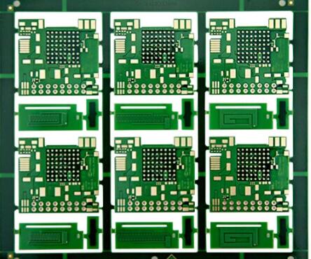
Method for making blind holes on HDI circuit board
The general HDI circuit board uses metalized blind holes to connect the various circuit layers that need to be connected. The production process includes: after a certain layer of copper foil layer is laminated, an etching process is used to process the blind holes that penetrate the copper foil layer. The diameter is generally not more than 0.2_; afterwards, the dielectric layer under the blind hole is removed by a laser ablation process to form a blind hole that reaches the upper copper foil layer; then, the blind hole is metalized to realize the two layers of copper foil. Interconnection; Then, you can continue to laminate the build-up layer, and use the same method to make metalized blind vias after the build-up, and use the same method to make the metalized blind vias after the build-up, so as to realize the interconnection between other layers.
The method for making blind holes on HDI circuit boards includes the following steps: 1. coating photosensitive epoxy resin; 2. baking the circuit board and curing the resin; 3. using the image transfer method to open the blind holes on the circuit board to remove the need for blind holes. The epoxy resin at the hole position makes the inner pattern copper pad stand out; 4. mechanically drilled through holes; 5. metallization plating; 6. chemical copper etching.
How to define SMD is the first difficulty in CAM production.

In the PCB production process, graphics transfer, etching and other factors will affect the final graphics. Therefore, we need to compensate the lines and SMD separately according to the customer's acceptance criteria in CAM production. If we do not define SMD correctly, parts of the finished product may appear SMD is too small.
Specific production steps:
1. Close the drilling layer corresponding to the blind hole and buried hole.
2. Define SMD
3. Use the FeaturesFilterpopup and Referenceselectionpopup functions to find the pads of the include blind holes from the top layer and the bottom layer, respectively, the moveot layer and the b layer.
4. Use the Referenceselectionpopup function on the t layer (the layer where the CSP pad is located) to select the 0.3mm pad that touches the blind hole and delete it. The 0.3mm pad in the CSP area of the top layer is also deleted. Then according to the customer design CSP pad size, location, number, make a CSP and define it as SMD, then copy the CSP pad to the TOP layer, and add the pad corresponding to the blind hole on the TOP layer. The b-layer is made in a similar way.
5. Find out other SMDs with missing definitions or multiple definitions based on the profile provided by the customer.
Plug hole and solder mask:
In the HDI laminated configuration, the secondary outer layer is generally made of RCC material, which has a thin medium thickness and low glue content. The process experimental data shows that if the thickness of the finished plate is greater than 0.8mm, the metallization groove is greater than or equal to 0.8mmX2.0mm, One of the three metalized holes is greater than or equal to 1.2mm, two sets of plug hole files must be made. That is, the holes are plugged twice, the inner layer is flattened with resin, and the outer layer is directly plugged with solder mask ink before the solder mask. During the solder mask manufacturing process, there are often vias that fall on or next to the SMD. The customer requires all vias to be plugged, so when the solder mask is exposed or exposed by half of the hole, it is easy to leak oil.