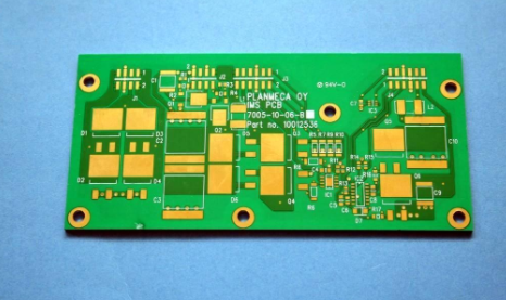
1. Device package inspection
We need to carefully check the motherboard device package to avoid errors. Especially for the newly used materials in the project, you must carefully check the PCB packaging with reference to the spec.
2. Component layout
When doing stacking, you need to consider the layout of structural parts and main components, such as I/O connector, SIM card, battery connector, T card, camera, speaker, receiver, RF part, baseband part, GSM antenna part, Bluetooth Antenna part, mobile TV antenna part. In addition to considering the ID and MD aspects, the placement of these parts also needs to consider the mutual influence.
In the MTK solution, the SIM card and the buttons are easily interfered by the GSM antenna, and it is necessary to stay away from the GSM antenna as much as possible. GSM antenna area, Bluetooth antenna area and mobile TV antenna area all need a suitable area. If the GSM is used as a PIFA antenna, it needs an area of 500mm2, and the antenna needs to be at least 5mm above the main board. There can be no I/O connectors, T cards, speakers and other devices under the antenna, otherwise the height can only be calculated from the height of the lower device to the antenna; if For monopole, the antenna space needs to be 30mm*10mm, the ground in this area on the motherboard needs to be hollowed out, and the antenna and the projection surface of the motherboard must not have metal. Speakers and receivers are susceptible to antenna interference, resulting in TDMA noise
, Need to consider their relative position to the antenna. The battery connector to the PA power supply also needs to be short. The position of the shielding cover of the radio frequency part given by Stacking, the radio frequency part can be used as a suitable whole to lay down the IQ line from the radio frequency part to the baseband part, the 26MHZ signal line, and the control line should be as short as possible and as smooth as possible. For the layout of the radio frequency part, it is necessary to straighten out the RX receiving line from FEM to tranceiver, the TX transmitting line from tranceiver to PA, and the TX transmitting line from PA to FEM or ASM.
The small filter capacitor of the power supply network should be as close as possible to the chip pin to reduce the lead inductance. Place other components in accordance with the principle of being nearby and by the way. The placement of components also needs to consider the height limit, in addition to considering the structural height limit, the height of the shielding cover will also limit the placement of the components. At present, the height of the two-piece shield is 1.8mm, and the height of the one-piece is 1.6mm. The height of the components in the RF shield must be within this range. If it is close to the periphery of the shielding cover, or on the ribs of the shielding cover, the height will be more restricted. The height of the main chip of the radio frequency part is 1.4mm, the height of FEM NTK5076 is 1.8mm, and the height of IMT0103B is 1.6mm. The height of the 47UF tantalum capacitor is 1.8mm.
3. The definition of each layer wiring
Before wiring, we need to determine the main ground layer, power layer, and roughly plan where the data lines, IQ lines, impedance lines, audio lines, high-frequency signal lines, control lines, etc. go.
Take the common 8-layer single-stage RF part single-sided ornamental motherboard as an example. The 8th layer is for device placement, the 1st layer is not displayed, the 6th layer is the auxiliary ground, and the 4th layer is the main ground. The power and data lines go to the 2nd and 3rd layers, and the TX and RX impedance lines go to the 8th layer as much as possible, and the 7th layer is hollowed out. Refer to the 6th layer. Try not to wire the 7th layer. IQ wires, audio wires, AFC, APC, 26MHZ, impedance wires, etc. are more susceptible to interference. Those who need special grounding can go to the 5th layer, and the upper and lower layers need to be grounded. The 4th layer is the main ground without wiring, and the 6th layer is the auxiliary ground, so try not to wire it.
4. Wiring specification
4.1 Impedance line
The impedance line should go to the surface layer as much as possible. When walking the surface layer, the lower layer should be hollowed out, and then the lower layer should be used as the reference ground. When walking the inner layer, the upper and lower layers need to be covered with ground for protection, and the left and right sides need to be covered with ground. For the 27 holes to be drilled, the 1st and 8th layers must be ground. Try to stay away from data lines, power lines, and signal lines to avoid interference. The TX impedance line is controlled to 50ohm, and the RX impedance line is currently a 150ohm differential line. The RX differential impedance control lines should be parallel, close, and equal in length.
4.2 High-frequency signal line
High-frequency signal lines, such as 26MHZ, EDCLK, etc., need to be protected with special grounding to avoid interference with GSM reception. Try to walk the inner layer and take the shortest distance. Both the upper and lower floors need to be covered with land. If you need to make 27 holes, make sure that the first and eighth layers of the 27 holes are grounded. High-frequency signal lines cannot be run near the antenna area.
4.3, APC, AFC, IQ lines and control lines to be protected
The IQ line needs special protection, usually the middle layer, such as the 5th layer. The upper and lower floors need to be ground. Copper protection should be laid on the left and right sides. Try to stay away from interference sources, such as power lines, data lines, high-frequency signal lines, etc. At the same time, avoid the 27 holes of the above interference sources that are too close to the IQ line. Since the IQ line is a differential line, it needs to be parallel, close, and equal in length. The IQ line is as straight as possible and the shortest distance. Both APC and AFC need to be covered separately, and the upper and lower layers need to be ground. Keep away from sources of interference. Other control lines, such as PA band-select, PA-enable, and FEM band-select lines, can be run together, as far as possible to cover the ground, and as far away as possible from the interference source.
4.4 Power and ground
The power supply wiring on the motherboard is very important. Try to make the entire power supply network star-shaped and avoid O-type power supply network to form a power loop and reduce EMC performance. When the PA is working, it consumes a lot of current. To avoid too much voltage drop of the PA input power, the PA's power supply line must be thick, and the general line width is 80mil. It is necessary to drill more mechanical holes and laser holes when changing layers. To make it fully connected, more holes are needed to connect with the battery connector. The VCCA and VCCB pin power cables of Skyworks PAsky77328 need to be pulled out separately from the battery connector, and the cable width is at least 16mil. The power supply to the triceiver also needs to be pulled out separately from the battery connector, with a line width of 16 mils. . The 26mhz crystal oscillator power supply is output from the PMU, and it also needs to be protected by a ground protection. The line width is 12mil. Other AVDD, DVDD, VCCRF, etc. can go 12mil. Except for PA power supply, at least 2 small holes for other power lines when changing layers. All power lines are sources of interference, so they should not be close to lines or devices that are susceptible to interference. Also not close to the high-frequency signal line, otherwise the high-frequency signal interference will spread over the entire motherboard along with the power line.
The ground of the battery connector and the ground of the main board should be fully connected. Make as many large holes as possible to the main ground to make it directly connected to the main ground. The more small holes are also better to ensure that the ground of each layer of the main board can be fully formed near the battery connector. Earth return. Make as many large holes as possible near the power cord to the main ground to make the loop area smaller and improve EMC performance. More small holes and large holes should be punched at the pads of the shielding frame to make it fully connected to the main ground. Make as many large and small holes as possible at the edge of the board to improve EMC performance. The PAD under the PA, FEM, and the transmitter has more large and small holes, which are fully connected to the main ground, and are beneficial for the PA to dissipate heat. Make more large and small holes under the 26MHZ crystal oscillator pad.
There are also several areas where copper paving needs to be prohibited.
1. GSM, BLUETOOTH, mobile phone TV and other antennas are broken, and copper is forbidden on floors 1 to 8. If it is a monopole antenna, it is forbidden to lay copper on the first to eighth floors of the entire antenna area.
2. There is no need to spread copper on the inner surface of the radio frequency shielding frame. If the radio frequency device is placed on the 8th layer, the ground of the 7th layer will be disconnected from the outer ground along the shielding frame and directly connected to the main ground by a large hole.
3. The ground below the 26MHZ crystal is also separated from the surrounding ground and directly connected to the main ground by a large hole.
In short, the more ground holes, the better, but if too many ground holes are intensively drilled in a large area with no traces, the board manufacturer may have opinions, and the PCB project may not be confirmed.
5. Productivity inspection
Check whether the components in the shielding case are too close to the shielding case to cause a short circuit. The safety distance is 12mil.
Check whether the device is too close to the edge of the board, which is easy to drop.
Check the solder mask layer, antenna pad, speaker PAD, RECEIVER PAD, vibration motor PAD, etc. to determine whether to apply tin.
Next, I will attach a series of precautions:
1. The RX line is a 150ohm differential impedance line. Adjust the line width according to the actual situation. It is required to be parallel, close, and equal in length.
2. The TX line is a 50ohm impedance line, adjust the line width according to the actual situation.
3, PA power supply, 80mil, need to punch more when changing layers. At least 2 large holes and 4 small holes.
4. PA VCCA, VCCB, need to take a line separately from the battery connector, the line width is 16mil.
5, 6129 power supply, you need to run a separate line from the battery connector, the line width is 16mil.
6, IQ line, walk 6mil, need to wrap the ground up, down, left and right. Need to be parallel, close, and equal length in pairs.
7. APC, AFC go 4mil, and the land needs to be well covered. The other control lines go 4mil, try to cover the ground.
8, FEM, PA, transceiver need to drill more ground holes.
9. The power lines of other RF parts are 16mil. When changing the layer, 2 small holes are required.
The 10,26MHZ signal line runs 4mil and needs to be covered with a good ground.
The above is the introduction to the key inspection part of the mobile phone PCB layout design. Ipcb is also provided to PCB manufacturers and PCB manufacturing technology.