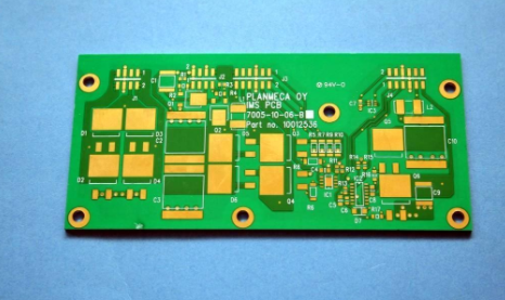
ENIG surface treatment of circuit board
The advantages of circuit board ENIG (nickel immersion gold) surface treatment
Its surface treatment can be used as the bottom metal of COB wire bonding.
Reflow (reflow) can be repeated many times, and it is generally required to be able to withstand at least 3 times of high temperature welding, and the welding quality can still be maintained.
Has excellent electrical conductivity. It can be used as a golden finger circuit for button conduction, and it has high reliability.
Gold metal has low activity and is not easy to react with the components in the atmosphere, so it can play a certain degree of anti-oxidation and anti-rust ability. Therefore, the shelf life of ENIG can generally easily exceed six months. Sometimes even if it is stored in the warehouse for more than one year, as long as it is kept in good condition and there is no rust problem, the circuit board is baked, dehumidified and soldered after testing. It is confirmed that there is no problem, and it can still be used for welding production.

Gold is not easy to oxidize when exposed to the air, so a large area of exposed pad can be designed for "heat dissipation".
It can be used as the contact surface of the blade. The gold layer for this application must be thicker. Hard gold plating is generally recommended.
The surface of ENIG is flat, the flatness of printed solder paste is good, and it is easy to solder. It is very suitable for fine inter-foot parts and small parts, such as BGA, Flip-Chip and other parts.
The disadvantages of circuit board ENIG (nickel immersion gold) surface treatment
Generally speaking, the solder joint strength of Ni3Sn4 is not as good as that of Cu6Sn5, and some parts that require soldering strength may not be able to withstand excessive external impact and risk of falling.
Because the price of gold is rising steadily, the cost is relatively higher than that of OSP surface treatment.
There is a risk of black pad or black nickel. Once the black pad is generated, it will cause the problem of a rapid decrease in the strength of the solder joint. The black pad is composed of a complex chemical formula of NixOy. The fundamental reason is that the nickel surface undergoes excessive oxidation during the immersion gold substitution reaction on the nickel surface (metal nickel becomes nickel ions, which can be called oxidation in a broad sense). Very large gold atoms (gold atom radius 144pm) are deposited irregularly to form a rough and loose porous crystal grain arrangement, that is to say, the gold layer cannot completely cover the nickel layer underneath, allowing the nickel layer to continue to be in contact with the air Finally, nickel rust gradually formed under the gold layer, which eventually caused welding hindrance. There is a nickel-impregnated palladium-gold (ENEPIG) process that can effectively solve the black pad problem, but because its cost is still relatively expensive, it is currently only used by high-end board, CSP or BGA companies.
iPCB is a high-tech manufacturing enterprise focusing on the development and production of high-precision PCBs. iPCB is happy to be your business partner. Our business goal is to become the most professional prototyping PCB manufacturer in the world. Mainly focus on microwave high frequency PCB, high frequency mixed pressure, ultra-high multi-layer IC testing, from 1+ to 6+ HDI, Anylayer HDI, IC Substrate, IC test board, rigid flexible PCB, ordinary multi-layer FR4 PCB, etc. Products are widely used in industry 4.0, communications, industrial control, digital, power, computers, automobiles, medical, aerospace, instrumentation, Internet of Things and other fields.