Circuit board solder mask and flux layer
Printed circuit boards{Printed circuit boards}, also known as printed circuit boards, are providers of electrical connections for electronic components.
Printed circuit boards are often represented by "PCB", but cannot be called "PCB boards".
Its development has a history of more than 100 years; its design is mainly layout design; the main advantage of using circuit boards is to greatly reduce wiring and assembly errors, and improve the level of automation and production labor.
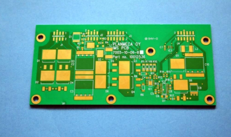
The difference between the solder mask and the solder flux layer of the circuit board
In the circuit board manufacturing process, what is solder mask? What is solder flux? And what is the difference between the two? In general, the group solder layer is mainly to prevent the direct exposure of the circuit board copper foil to the air. The role of protection, and the soldering layer is used as a stencil. When soldering, the solder paste can be accurately placed on the patch pads that need to be soldered.

The difference between the solder mask and the solder flux layer of the circuit board
he resistance pad is the solder mask, which refers to the part of the PCB that needs to be painted with green oil. In fact, this solder mask uses a negative output, so after the shape of the solder mask is mapped to the board, it is not the green solder mask, but the copper skin is exposed. Usually in order to increase the thickness of the copper skin, the solder mask is used to scribe lines to remove the green oil, and then tin is added to increase the thickness of the copper wire.
The soldering layer is used when the machine is patched, and corresponds to the pad of the patch component. In SMT processing, a steel plate is usually used, and the PCB corresponding to the component pad is punched, and then solder paste is placed on the steel plate., When the PCB is under the steel plate, the solder paste leaks, and it happens that every pad can be stained with solder, so usually the solder mask cannot be larger than the actual pad size.
Both layers are used for soldering. It does not mean that one is soldered and the other is green oil, but:
1. The soldering layer is used for chip packaging.
2, by default, the area without solder mask should be painted with green oil;
3. The meaning of the solder mask is to open a window on the green oil of the whole solder mask, the purpose is to allow welding;
iPCB is a high-tech manufacturing enterprise focusing on the development and production of high-precision PCBs. iPCB is happy to be your business partner. Our business goal is to become the most professional prototyping PCB manufacturer in the world. Mainly focus on microwave high frequency PCB, high frequency mixed pressure, ultra-high multi-layer IC testing, from 1+ to 6+ HDI, Anylayer HDI, IC Substrate, IC test board, rigid flexible PCB, ordinary multi-layer FR4 PCB, etc. Products are widely used in industry 4.0, communications, industrial control, digital, power, computers, automobiles, medical, aerospace, instrumentation, Internet of Things and other fields.