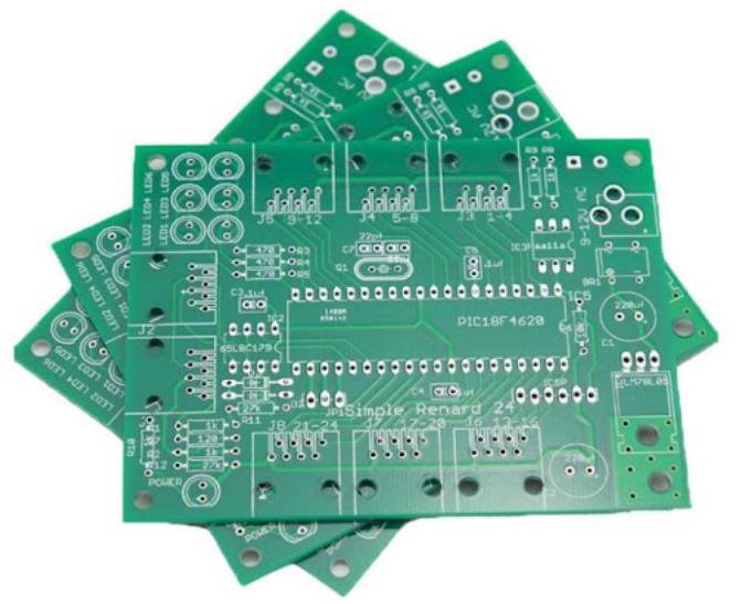
Circuit board PCB proofing urgent
What quality problems are easy to cause if the circuit board PCB proofing is urgent?
1. The thickness of the pad coating is not enough, resulting in poor soldering. The thickness of the pad surface of the component that needs to be mounted is not enough. For example, if the tin thickness is not enough, it will cause insufficient tin when melting at high temperatures, and the components and pads cannot be well soldered.
2. The surface of the pad is dirty, which will cause the tin layer to not wet; if the surface of the board is not cleaned, such as the gold plate has not been cleaned, it will cause too much impurities on the surface of the pad, resulting in poor soldering.
3. The pad on the wet film is offset, which will cause poor soldering, and the pad on the wet film that needs to be mounted on the component will also cause poor soldering.

4. The pad is defective, which will cause the component to be unable to be soldered or the soldering is not strong.
5. BGA pads are not developed cleanly, and residual wet film or impurities will cause the solder to fail to be soldered during mounting. The protruding plug hole at the BGA leads to insufficient contact between the BGA component and the pad, which is easy to open. If the solder mask at the BGA is too large, copper will be exposed on the line connected to the pad and the BGA patch will be short-circuited.
6. The spacing between positioning holes and patterns does not meet the requirements, causing the printed solder paste to be offset and short-circuited.
7. The green oil bridge between IC pads with dense IC pins is broken, resulting in poor printed solder paste and short circuit. The via plug next to the IC is protruding, causing the IC to fail to mount.
8. The stamp hole between the units is broken and solder paste cannot be printed. Drilling the identification light spot corresponding to the wrong fork board will cause waste when automatically pasting the part. The second drilling of the NPTH hole will cause a relatively large deviation in the positioning hole, which will cause the printed solder paste to shift.
9. Ensure that the light spots are neat, matte and without gaps. Otherwise, the machine is difficult to identify smoothly and cannot automatically attach parts, and the mobile phone board does not support re-sinking nickel, otherwise it will cause serious unevenness in nickel thickness.
iPCB is a high-tech manufacturing enterprise focusing on the development and production of high-precision PCBs. iPCB is happy to be your business partner. Our business goal is to become the most professional prototyping PCB manufacturer in the world. Mainly focus on microwave high frequency PCB, high frequency mixed pressure, ultra-high multi-layer IC testing, from 1+ to 6+ HDI, Anylayer HDI, IC Substrate, IC test board,rigid flexible PCB, ordinary multi-layer FR4 PCB, etc. Products are widely used in industry 4.0, communications, industrial control, digital, power, computers, automobiles, medical, aerospace, instrumentation, Internet of Things and other fields.