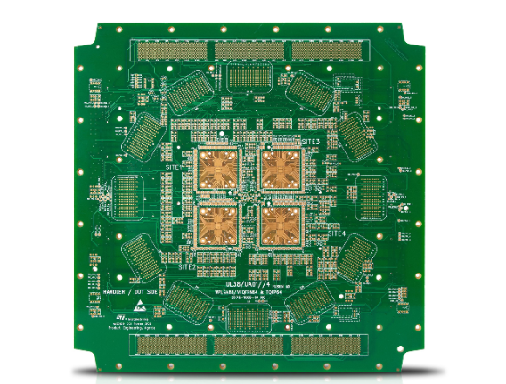
What is HDI (High Density Interconnect) PCB circuit board
High Density Interconnect (HDI) PCB is a technology for the production of printed circuit boards. It is a circuit board with a relatively high line distribution density that uses micro-blind via and buried via technology. With the continuous development of science and technology, in order to meet the electrical requirements of high-speed signals, the circuit board must provide impedance control with alternating current characteristics, high-frequency transmission capabilities, and reduction of unnecessary radiation (EMI). Sometimes in order to reduce the quality of signal transmission, insulating materials with low dielectric coefficient and low attenuation rate are generally used. In order to better match the miniaturization and arraying of electronic components, circuit boards are constantly increasing in density to meet compliance requirements.

HDI (High Density Interconnect) circuit boards include laser blind vias and mechanical blind vias; in order to achieve the technology of conduction between the inner and outer layers, generally through and buried vias, blind vias, stacked vias, staggered vias, cross blind buried, vias, Blind hole filling electroplating, fine line and small gap, micro-hole in the disk and other processes are realized.
HDI circuit board can be divided into: 1st order, 2nd order, 3rd order, 4th order and any layer interconnection
1st order HDI structure: 1+N+1 (2 times of pressing, 1 time of laser)
2nd order HDI structure: 2+N+2 (3 times of pressing, 2 times of laser)
3 level HDI structure: 3+N+3 (4 times of pressing, 3 times of laser)
4th order HDI structure: 4+N+4 (5 times of pressing, 4 times of laser)
From the above structure, it can be concluded that the laser is a first-stage board once, twice is a second-stage board, and so on.
At present, the HDI circuit boards that can be used in batches for multi-layer circuits are mainly within the 3rd order. The 4th order and any layer interconnection is limited to small batch sample production. At present, we are intensifying research and development. I believe that the 4th order HDI board and any layer interconnection will be in the near future. Will be mass produced.
Electronic design is constantly improving the performance of the whole machine, while also working hard to reduce its size. In small portable products ranging from mobile phones to smart weapons, "small" is an eternal pursuit. High-density integration (HDI) technology can make terminal product designs more compact, while also meeting higher standards of electronic performance and efficiency. HDI is currently widely used in digital products, such as mobile phones, digital (camcorder) cameras, MP3, MP4, notebook computers, automotive electronics, etc., and mobile phones are the most widely used. HDI boards are usually manufactured by build-up. As the number of build-ups increases, the technical level of the board will be higher. The general HDI board is basically one-time build-up, and high-end HDI uses advanced PCB technology such as two or more build-up techniques, stacking holes, electroplating and filling holes, and laser direct drilling. High-end HDI boards are mainly used in 3G mobile phones, digital cameras, IC carrier boards, etc.