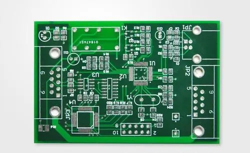
Below I will introduce my understanding of the motherboard. If you don’t speak well, please give me some advice:

First of all, you should set Space and some line widths for some important signals before making the picture. If the customer does not have Layoutguide, we must have experience in this area. In general, we should pay attention to the basic routing rules of the following signals:
1. DDR signal:
In addition to the Control line, DDR lines are generally 5/10 Control lines to maintain a line spacing of 20mil. Like the CPU, they are mainly divided into the following three categories:
<1>Data lines (0-63) 64 lines
<2>Address line (0-13) There are also some address signal lines with other names,
<3>Control line (generally distributed in the middle of the data and address lines)
When the data lines are routed, each 8 lines are a group, plus 2 DQM and DQS control lines to go together and go on the same layer. The main grouping methods are:
MD (0-7) add DQM0 DQS0
MD (8-15) plus DQM 1 DQS 1
MD (16-23) plus DQM 2 DQS 2
MD (24-31) plus DQM3 DQS 3
MD (32-39) plus DQM 4 DQS 4
MD (40-47) plus DQM 5 DQS 5
MD (48-55) plus DQM 6 DQS 6
MD (56-63) plus DQM 7 DQS 7
Try to keep all Address lines together;
In addition, there are 3 pairs of CLK lines in the DDR part. If it is a dual-channel DDR, there are 6 pairs of CLK lines. The CLK should be paired and kept at least 20 mils apart from other signals.
DDR and CPU should also be separated from other signals with a 20-30mil GND signal, mainly the signals of CPU and AGP
2. CPU wiring:
In general, the CPU wiring is to use 5/10 Control line spacing to be slightly larger, about 20mil,
<1> 64 data lines (0-63);
<2>Address line (3-31) REQ (0-4), etc.
<3>Control line (generally distributed in the middle of the data line and the address line)
When the data lines are routed, every 16 lines are grouped together and run on the same layer.
(0-15) (16-31) (32-47) (48-63) and each group distributes 2-3 control lines,
When the Address lines are routed, every 16 lines are grouped together and run in the same layer. The difference is that the Address lines are not from (3-31) before (0-2). Generally divided into 2 groups,
<1> (3-16) Add 5 REQ wires, 18;
<2> (17-31) 16 pieces;
When routing the CPU signal, it should also be separated from other signals with a 20-30mil GND line, such as DDR signals, to facilitate the GND under the VIA and play a role in the ground.
3. CLK signal:
The CLK signal is the most important signal in the motherboard, generally as large as the following:
<1>200 trillion
<2>100 trillion
<3>66 trillion
<4>48 trillion
<5>16 trillion
Generally, the first two types are mainly used for CPU and NB. They are high-frequency CLK lines and should be kept at least 25 mils apart.
The third type is mainly used in DDR and SB, 20/7/5/7/20,
The fourth type is generally used in PCI and AGP, 20/7/5/7/20,
The fifth type is generally seldom used, mainly for some small IC. and AUDIO parts. Compared with the previous types, this CLK is slightly less important. Just go 15/5/15. The CLK signal should also be used. Use less vias, generally not more than 2 VAI. When routing, try to refer to GND. Crystal oscillators cannot be routed on the component side, and the signal of the crystal oscillator should be as short as possible.
4. LAN signal:
LAN, the signal generally has 2 pairs of signals, paired to go, 20/7/5/7/20 or 20/10/10/10/20.
Try to refer to the GND layer when routing. Play less VAI and try not to exceed 2 vias.
5. AUDIO signal:
The AUDIO signal is generally 10/10, and generally cannot pass through other signal areas, and other signal areas cannot pass through the AUDIO area.
6. USB signal:
For USB1.0, go 10/10/10. It can be more than 20mil empty with other signals;
For USB2.0, go 7.5/7.5/7.5 and other signals with a space of more than 20mil;
Try to refer to the GND layer when routing. Play less VAI, try not to exceed 2 VAI.
7. VLINK signal
VLINK signals generally have 11 data lines and 2 control lines. If the two control lines are paired, the spacing between VLINK signals should be larger, at least 15 mils or more, and the distance between the 2 paired lines and other VLINK signals should be 20 mils. No more than 2 vias, and land should be covered.
8. PCI signal:
PCI signal requirements are not so high, just go 5/5/5.
9. IDE signal:
IDE signals mainly include (pd0-15) 16 wires plus 2 control wires, and some other signal wires. The control wires are generally 25pin, and 27pin, and Space can go 10/5/10.
10. Power signal:
Pay attention to the line width when routing the power signal. The main purpose is to distinguish the source of the power supply and the amount of current. Generally, we can use a 40mil line width for 1A. When the line width is not enough, you can consider laying copper or cutting to the inner layer. The signal goes too close.
The above points have almost introduced my understanding of this skill. I will continue to work hard to further understand and understand various types of signals and wiring requirements.
The above is the introduction to the wiring requirements of the computer motherboard. Ipcb also provides PCB manufacturers and PCB manufacturing technology.