The outer frame (clamping side) of the PCB jigsaw should adopt a closed-loop design to ensure that the PCB jigsaw will not be deformed after being fixed on the fixture
2. The center distance between the small plates is controlled between 75 mm and 145 mm

3. The PCB board shape should be as close to the square as possible, and 2*2, 3*3,..., and...
4. Four positioning holes are made at the four corners of the frame of the jigsaw, with a diameter of 4mm±0.01mm; the strength of the holes should be moderate to ensure that they will not break during the upper and lower boards; the precision of the hole diameter and position should be high, and the hole wall should be smooth and without thorns
5. There should be no large devices or protruding devices near the connection points between the outer frame of the jigsaw and the inner small board, and the small board and the small board, and there should be more than 0.5mm space between the components and the edge of the PCB to ensure The cutting tool is operating normally
6. Each small board in the PCB puzzle board must have at least three positioning holes, 3≤aperture≤6 mm, and no wiring or patching is allowed within 1mm of the edge positioning hole
8. The reference symbols used for the positioning of the entire PCB and the positioning of fine-pitch devices. In principle, the QFP with a spacing of less than 0.65mm should be set in its diagonal position; the positioning reference symbols used for the imposition PCB daughter board should be used in pairs, Arranged at the opposite corner of the positioning feature.
9. When setting the reference anchor point, usually leave a non-solder mask area 1.5 mm larger than it around the anchor point
10. PCB panel width ≤260mm (SIEMENS line) or ≤300mm (FUJI line); if automatic dispensing is required, PCB panel width*length ≤125 mm*180 mm
11 large components should have positioning posts or positioning holes, such as I/O interface, microphone, battery interface, micro switch, earphone interface, motor, etc.
12. I/O ports, headphone jacks and side keys should not be spliced as much as possible, and the splicing position should be selected in a straight line or a position with a large arc as far as possible, which is conducive to processing
13. The positioning hole of the clamping edge should be more than 4-5mm from the edge of the board
14.Usually the entire PCB is rectangular. Considering the weight bearing of PCB components, the short side and the board side are added.
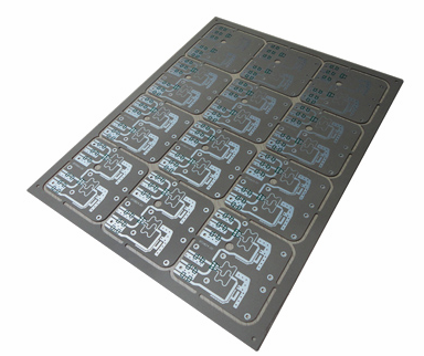
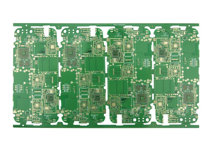
15. The number of puzzle pieces is evaluated according to the convenience of actual work.
16.It is usually necessary to pay attention to whether there are connectors and other interference between the panels.
17.AI and SMD boards are usually used, and the sides of the board are reserved for 5m~6m, and two 4*6mm positioning holes are placed on each side.
The above is an introduction to the points that need to be paid attention to in PCB assembly. Ipcb is also provided to PCB manufacturers and PCB manufacturing technology.