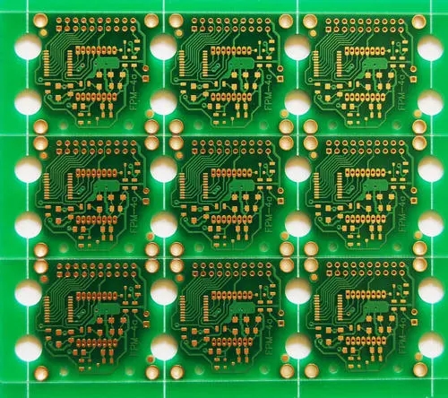
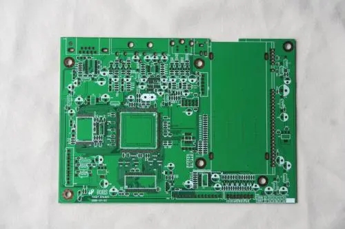
There was no special PCB layout before, especially for mobile phones. At the beginning, I felt that there was nothing, but in the end, I was really going crazy. There is no way out. real! The boss started talking about 6 days. Starting from the layout, I wonder if the boss is crazy. Some colleagues actually said yes! I really want to cut people with a kitchen knife. Later, the boss said: "It’s a bit tight, or else, two people will do it together. I rely on, the boss is really creative. There is no way to call me a part-time job. Just like this, my most painful and long PCB LAYOUT began. In addition, there has been no REST for 6 weeks a few days ago, and now it’s fine. It’s cool to go to work at night! Cool!

Now I really don’t want to live!
Don't say you have done it better than not doing it well, even if it is unsuccessful.
Stop talking nonsense, let me talk about my experience first. If there are professionals, experts or senior engineers here, please give us more opinions and suggestions!
I use POWER PCB 5.0.
1. The thread ends first
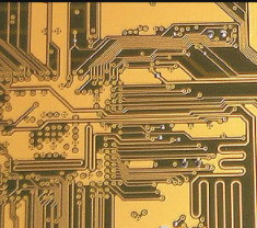
2. Tightly trace
3. The upper and lower wires should overlap as much as possible, leaving room for punching holes
4. Do not block the road when routing, give the surrounding space as much as possible
5. The punching area and wiring area can be separated
6. Except for GND, make fewer through holes.
7. Less wiring in the lower layer of the IC
8. To be proficient in the use of tools, functions and quick decision keys
9. Do not run wires on the holes
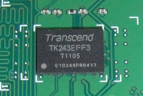
10. If necessary, holes can be punched on the BGA pads
11. The layout is very important, analyze the density and direction of the flying line (the principle of proximity)
12. You can go close to the peripheral devices first (if there is a flying line, you can walk on the peripheral device, and try to make as little as possible)
13. If there are multiple connections, look wherever is near and convenient, then go where
14. After punching under the IC, it is best to walk closer to the IC boundary
15. Try to go to the surface as far as possible in the short-term.
16. When wiring, the corresponding schematic diagram, it is best to print it out
17. First take the line that is close to the IC on the surface layer, so that you can make holes there. (No worries)
18. When laying out, the ones that can be placed closer must be placed closer, especially around the BGA, the layout is the first, the pattern is second, and the beauty is third.
19. Wiring is a systematic task, it is best to be done by one person, if there is more than one, it will lead to death.
20. If you can plan the basket, you must consider the margin and strive for space.
21. When making the schematic diagram, it must be concise and clear, with fewer components, high integration, and sealed, small, optional components must be removed.
22. Distinguish which lines are set or settable (there is no other way to move) should go first, and move later.
23. If possible, leave the trace width between devices during layout.
24. Three-dimensional lines should be used for large-scale BGA ICs (multi-layers). Do not use flat surfaces (all on the same layer). You will know what it means later.
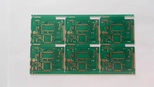
The above is the introduction of mobile phone PCB LAYOUT design experience, Ipcb also provides PCB manufacturers and PCB manufacturing technology.