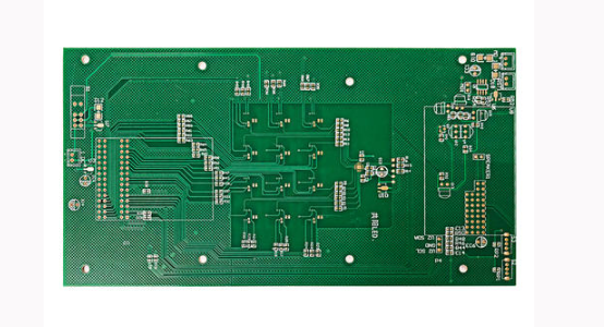
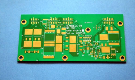
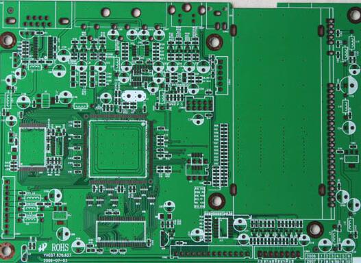
The word mark on the PCB circuit board is like the birthmark on our human beings, it is the mark from the mother's womb. It is used on the circuit board to clearly mark the standard version number of the PCB design and the position symbol of each electronic component; it is made by the PCB manufacturer during the process of making the plate; it plays an important reference in the SMT mounting and soldering process effect. In the "life" of the circuit board, it has to go through the various tests of blood and fire together with the circuit board and stand upright, and it can be regarded as a real "man".

It is as important as our circuit boards and printed metal circuit lines, and no "magic ghosts" can be caused here.
Common PCB markings have etching marking oil and ink markings. Let's follow the footsteps of the Canadians to see what quality control standards they have.
1. Etching marks
The production of etching marks is the same as the production of conductors on the printed board. Therefore, the etching mark should meet the following requirements.
•Each character is legible.
• Maintain minimum conductor spacing requirements between etched characters and active conductors.
• In the case of legible characters, marking defects (such as solder bridging, over-etching, etc.) are acceptable.
• The mark does not violate the minimum electrical clearance requirements.
• When the general meaning of a character or mark can be distinguished, the edges of the character appear slightly irregular.
• The defect does not meet or exceed the above requirements.
2. Ink marking
Ink mark refers to any type of mark printed on the surface of the printed board. The production of this type of mark must not involve cutting or etching.
• The ink is evenly distributed without blurring or ghosting.
• The ink mark is at most tangent to the connecting plate.
• The characters are legible.
• As long as the characters are recognizable, the ink can be accumulated outside the character lines.
• As long as the required orientation is still clear and clear, the outline of the component orientation symbol shown in the figure below can be partially peeled off.
• The marking ink of the component hole connecting plate shall not penetrate into the component mounting hole, or cause the ring width to be lower than the minimum ring width.
• Unless the procurement documents require that the holes be completely filled with solder, marking inks are allowed in the plated holes and via holes that do not solder component leads.
• The marking ink does not encroach on the printed contact sheet or the surface of the test point on the edge of the board.
• For surface mount connection disks with a pitch greater than or equal to 1.25 mm [0.04921 in], ink can only encroach on the tip of the iceberg, and the pool must not be half-year-old (0.05 mm [0.0020 in]).
• For surface mount lands with a pitch of less than 1.25 mm [0.04921 in], the ink can only invade one side of the lands, and no more than 0.025 mm [0.000984 in].
![PCB design process [turn] [PCB technology]](/public/upload/image/20211101/02dcafe72b0ee319f6836d490bab9a17.jpg)