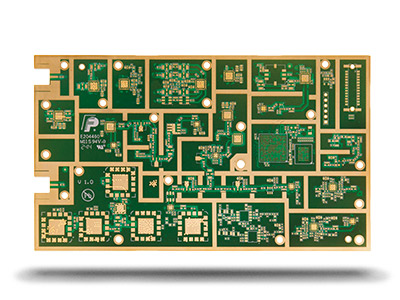
A, let's introduce Immersion gold(ENIG).
The copper on the circuit board is mainly red copper, and the copper solder joint is easy to be oxidized in the air, which will cause poor conductivity, that is, poor tin eating or poor contact, and reduce the performance of the circuit board, so it is necessary to carry out surface treatment on the copper solder joint. A gold deposition is plating gold on it, which can effectively block the copper metal and the air to prevent oxidation, so gold deposition is a treatment method for surface oxidation prevention, It is a chemical reaction that covers the surface of copper with a layer of gold, also known as Immersion Gold.
.jpg")
B, what is Golden Finger?
Brass contacts can also be said to be conductors. In detail, it refers to the components connected with the memory socket on the memory module. All signals are transmitted through gold fingers. It is composed of many yellow conductive contacts. Its surface is gold-plated and the conductive contacts are arranged like fingers, so it is named Gold Finger.
The advantage of the gold deposition process is that the deposition color on the surface of the printed circuit is very stable, the brightness is excellent, the coating is very flat, and the weldability is excellent. Generally, the thickness of gold precipitation is 1-3 inches, which can be basically divided into four stages: pretreatment (oil removal, micro etching, activation, post immersion), nickel precipitation, gold precipitation, and post-treatment (waste gold washing, di washing, drying).
However, compared with other tin spraying processes, the cost of the gold deposition process is relatively high. If the thickness of gold exceeds the conventional process of the plate factory, the cost is even more expensive. Of course, if you have high requirements for the weldability and electrical properties of the board, it is another matter. For example, if your circuit board has gold fingers that need to be sunk or the line width/pad spacing of the board is insufficient, it is best to do the process of sinking gold + gold-plated fingers so that the circuit board welding is very good, the performance of the circuit board is also very stable, the pad will not fall off, the contact will not be bad, there will be no short circuit and other phenomena, and it is also very shockproof and fall-proof. Of course, we will not fall the board.
There is also a case where the circuit board has gold fingers, but the plate surface other than the gold fingers can choose the tin spraying process according to the situation, that is, the tin spraying + gold-plated finger process. When the circuit board width and pad spacing are sufficient and the welding requirements are not high, it can effectively reduce the manufacturing cost without affecting the use of the board. However, if the line width of the board and the spacing between the pads are insufficient, the tin spraying process will increase the production difficulty. There will be more short circuits such as tin bridging, and there will also be frequent insertion and stripping of gold fingers, resulting in poor contact.
Therefore, we can choose the suitable board-making process according to the actual situation of our own circuit board, that is, we can control the cost without affecting the use of the board.

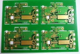
Gold Finger
A gold deposition is one of the surface treatment processes of PCB. It uses the chemical deposition method to generate a layer of the coating through a chemical oxidation-reduction reaction, which is usually relatively thick. It belongs to a method of chemical nickel gold deposition, which can achieve a thicker gold layer.
What should I do if the gold-plated PCB is not tin-plated? To solve the problem, first of all, we need to analyze the reasons why the gold-plated PCB can't be coated with tin, mainly including the following points:
(1) Tin failure caused by PCB oxidation;
(2) The temperature of the furnace is too low or the speed is too fast, and the tin does not melt;
(3) If there is a problem with the solder paste itself, you can try another solder paste;
(4) There is a problem with the battery, because the battery is usually stainless steel, and it needs to be plated with a layer of chromium before tin can be applied.
Knowing the reason why the gold-plated PCB can't be coated with tin, let's talk about the solution, as follows:
(1) Regularly test and analyze the components of the liquid medicine, timely add, increase the current density, and extend the electroplating time.
(2) Check the consumption of anode from time to time and make reasonable supplements;
(3) Reasonably adjust the distribution of the anode, appropriately reduce the current density, reasonably design the wiring or splicing of the board, and adjust the brightener;
(4) Strictly control the storage time and environmental conditions in the storage process, and strictly operate the manufacturing process;
(5) Use solvent to clean sundries. If it is silicone oil, it needs to be washed with a special cleaning solvent;
(6) During PCB welding, the temperature should be controlled at 55-80 ℃, and sufficient preheating time should be ensured.
A gold finger is a row of equidistant square pads on a PCB circuit board, exposed copper and gold plating; It is commonly used for electrical connection pins of boards, LCD connections, mainboards, chassis, and other connections. So, what are the categories of PCB gold fingers?

1. Definition and function of a golden finger:
Gold finger, insert one end of the PCB circuit board into the connector card slot, and use the insertion pin of the connector as the outlet of the circuit board to make the pad or copper skin contact with the pin at the corresponding position. In order to achieve the purpose of orientation, a nickel gold plate is plated on the pad or copper skin on the PCB board, which is called a gold finger because of the shape of the finger. Gold was chosen because of its superior conductivity and oxidation resistance. Wear resistance.
2. Classification and recognition characteristics of golden fingers:
Gold fingers are divided into ordinary gold fingers (flat fingers), segmented gold fingers (intermittent gold fingers), and long and short gold fingers (uneven gold fingers).
(1) Ordinary gold fingers: arranged on the edge of the board in a neat manner, with the same length and width as the rectangular pad.
(2) Segmented golden finger: rectangular pad, whose length is different on the edge of the board, and the front section has been disconnected;
(3) Long and short gold fingers: rectangular pads with different lengths located at the edge of the PCB board.