1.
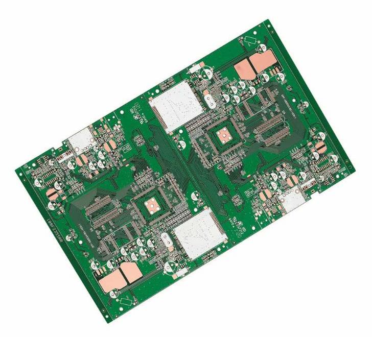
PCB board can be structurally divided into single-sided, double-sided and multi-layer boards.
Among them, a multi-layer board refers to a printed board with more than two layers, which is composed of connecting wires on several layers of insulating substrates and pads for assembling and soldering electronic components. The role of high-speed PCB boards is generally designed with multi-layer boards. Common multi-layer boards are generally 4-layer boards or 6-layer boards, and complex multi-layer boards can reach dozens of layers.
2, the characteristics of PCB board multilayer board
The difference between the multi-layer PCB board and the single-sided and double-sided boards is that the internal power supply layer (maintaining the internal electrical layer) and the grounding layer are added. The power supply and grounding network are mainly routed on the power supply layer. However, the multi-layer board wiring is mainly based on the top layer and the bottom layer, supplemented by the middle wiring layer.
Multilayer PCB boards are mainly composed of the following layers: Signal Layers, InternalPlanes Layers, Mechanical Layers, Sloder Mask Layers, Silkscreen Layers, and System Layers.
Multilayer PCB boards have many advantages, such as: high assembly density and small size; shortened connections between electronic components, fast signal transmission speed, convenient wiring; good shielding effect and so on.
3. Design of multi-layer
PCB board
Each layer should be symmetrical, and it is an even number of copper layers. If it is not symmetrical, it is easy to cause distortion. The wiring of the multilayer board is carried out according to the circuit function. When wiring the outer layer, it is required to have more wiring on the welding surface and less wiring on the component surface, which is beneficial to the maintenance and troubleshooting of the printed board. In terms of wiring, it is necessary to separate the power supply layer, ground layer and signal layer to reduce the interference between power supply, ground and signal. The lines of the two adjacent layers of printed boards should be perpendicular to each other as much as possible or follow oblique lines and curves, but not parallel lines, so as to reduce the interlayer coupling and interference of the substrate.
4. Determination of board shape, size and number of layers
The shape and size of the printed board must be based on the overall structure of the product. From the perspective of production technology, it should be as simple as possible, generally a rectangle with a not very disparate aspect ratio, so as to facilitate assembly, improve production efficiency and reduce labor costs.
In terms of the number of layers, it must be determined according to the requirements of circuit performance, board size and circuit density. For multi-layer printed boards, four-layer boards and six-layer boards are widely used.
The layers of the multi-layer board should be kept symmetrical, and it is an even number of copper layers, that is, four, six, eight layers, etc. Because of the asymmetric lamination, the board surface is prone to warpage, especially for surface mount multilayer boards, which should be paid attention to.
5. Position and orientation of components
The position and placement direction of components should first be considered from the perspective of circuit principles and cater to the trend of the circuit. Whether the placement is reasonable or not will directly affect the performance of the printed board, especially for high-frequency analog circuits, the requirements for the location and placement of components are obviously more stringent. Therefore, when engineers start to arrange the layout of the printed board and decide the overall layout, they should conduct a detailed analysis of the circuit principle, first determine the location of special components (such as large-scale ICs, high-power transistors, signal sources, etc.), and then Arrange other components and try to avoid factors that may cause interference. On the other hand, the overall structure of the printed board should be considered to avoid uneven arrangement of components and disorder. This not only affects the appearance of the printed board, but also brings a lot of inconvenience to assembly and maintenance work.
6. Requirements for wire layout and wiring area
In general, multi-layer printed board wiring is carried out according to circuit functions. When wiring the outer layer, it is required to have more wiring on the welding surface and less wiring on the component surface, which is beneficial to the maintenance and troubleshooting of the printed board. Thin, dense wires and signal lines that are susceptible to interference are usually arranged on the inner layer. A large area of copper foil should be distributed evenly in the inner and outer layers, which will help reduce the warpage of the board and also enable a more uniform coating on the surface during electroplating. In order to prevent damage to the printed wires and short circuits between layers during machining, the distance between the conductive patterns in the inner and outer wiring areas and the edge of the board should be greater than 50 mils.
7. Requirements for the direction of the wire
The multi-layer board traces should separate the power layer, the ground layer and the signal layer to reduce the interference between the power, ground and signal. The lines of the two adjacent layers of printed boards should be perpendicular to each other as much as possible or follow oblique lines and curves, but not parallel lines, so as to reduce the interlayer coupling and interference of the substrate. And the wire should be as short as possible, especially for small signal circuits, the shorter the wire, the smaller the resistance and the less interference.
8. Requirements for safe distance
The setting of the safety distance should meet the requirements of electrical safety. Generally speaking, the spacing of outer conductors should not be less than 4 mils, and the spacing of inner conductors should not be less than 4 mils. In the case that the wiring can be arranged, the spacing should be as large as possible to improve the yield of the board and reduce the hidden danger of failure of the finished board.
9. Requirements for improving the anti-interference ability of the whole board
In the design of multi-layer printed boards, we must also pay attention to the anti-interference ability of the entire board. Add filter capacitors near the power supply and ground of each IC, and the capacity is generally 473 or 104. For sensitive signals on the printed board, the accompanying shielded wires should be added separately, and the wiring should be as little as possible near the signal source. Choose a reasonable grounding point on
PCB board.