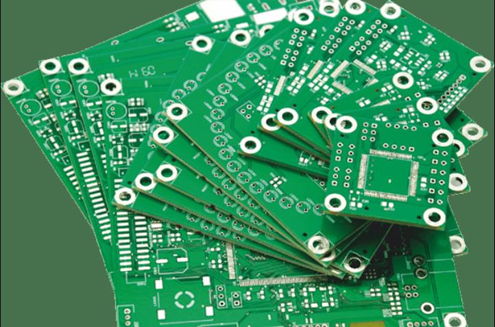
PCB board layout designers are generally not involved in planning the layer stackup used to build the circuit board they are designing. In order to set up the design tool, they obviously have to know the correct number of layers and their configuration, but beyond that, they won't have any further interaction. This is mainly due to three reasons: The performance requirements of PCB boards are not as stringent as they are now. Less material is used to make PCB boards. PCB board design tools simply do not have the complex layer stack-up and configuration capabilities of today. Thankfully, this part of the PCB board layout process is very different now, as most major design tools are equipped with advanced PCB layer configuration capabilities. Having said that, designers are still responsible for completing the process of configuring the correct ply stack-up for their designs. We'll look at the process and discuss some ideas for building and configuring layer stacks in PCB board design software.

The number of layers on printed circuit boards are directly related to the number of nets that need to be routed. With the increase in the circuit demand of the PCB board, the number of components also increases, and the number of final nets also increases. At the same time, the complexity and pin count of active components is also increasing, which increases the net count on the board. The answer to these increases is to reduce the trace width or increase the number of layers on the board, or both, which unfortunately leads to higher manufacturing costs. While the average and net number of components on a PCB board has increased, so has the board's electrical performance metrics. Designers quickly discovered that while routing previously required four layers instead of six, they actually had to reach eight layers to achieve the desired electrical performance. Some reasons for these additional layers include:
1) More room for isolated controlled impedance routing.
2) Differential pair routing is limited to as few layers as possible.
3) Microstrip and stripline layer stack configuration.
4) Additional plane layers for multiple power and ground nets.
As board functionality continues to evolve, another factor is introduced into the process of creating a board layer stackup. The higher operating speeds of today's circuit boards may require more circuit board fabrication material than previously used circuit boards. The same goes for high power boards or boards that will be used in harsh environments. These materials may change the transmission line properties of circuits originally calculated for standard FR-4 materials, which may in turn require changes to the layer stacking configuration.
With today's advanced electronics, it is critical to create the correct board layer stackup to ensure that the board will perform at its high performance. And since we've just discussed all the requirements, layout designers are under more pressure than ever to get the stacking right. Let's see what other difficulties layout designers face. The need to bring products to market is now more urgent than ever. Not only are companies facing greater competitive pressure, but other forces are at play. For example, the recent COVID-19 outbreak has created a frenzy for medical design efforts to bring new medical devices into production to help fight the virus. While all aspects of design feel the pressure to meet these demands, PCB board designers in particular face the challenge of getting boards to complete quickly and without errors. As we pointed out before, the requirements for layer configurations and board materials are becoming more and more complex every day. Many designers are unfamiliar with all of these processes or materials and need outside help to create the right ply stack for their design. Some PCB board design tools are still not user-friendly enough for designers to use effectively when creating their PCB board stack-ups. Not only does this slow down and increase the frustration of work, but it can also affect the design level of the board. PCB board layout designers face many challenges when trying to get the job done. This is especially true when trying to create a board stack-up configuration to ensure the board works as expected, while being able to manufacture the board without errors and at a cost. Let's take a look at some of the ways that PCB board design tools can help designers. PCB board CAD tools can do many things to help layout designers create and configure board layer stackups. The first is to incorporate an automatic generator or wizard, as shown in the image above. These tools allow designers to specify the number of layers and configuration of the stack, which requires extensive creation in the database. Next comes the ability to give the designer full control over the details of the layer stack-up, including the ability to specify conductive and dielectric plate materials. Designers should be able to specify values and tolerances, and configure how layers should be laid out when setting layout parameters. But not all the help designers need come from these tools. Designers need to have a lot of industry knowledge to better understand the materials and processes they work with. Here, designers can benefit greatly by developing relationships with PCB board contract manufacturers to obtain accurate information for creating their board layer stack-ups. As already said, manufacturers have been doing this for years and they are very good at it. Layout designers should be encouraged to participate in their PCB board CM early in order to have the correct lay-up before they begin PCB board design.