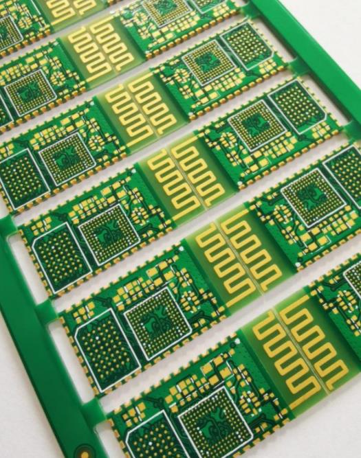
1. PCB board surface treatment
The surface treatment processes for PCB boards include: oxidation resistance, tin spraying, lead-free tin spraying, enig, tin precipitation, silver precipitation, hard gold plating, full board plating gold, gold fingers, nickel palladium OSP, etc. The main requirements are: low cost, good weldability, harsh storage conditions, short time, environmentally friendly process, good welding, and flatness. Tin spray: Tin spray panels are generally multi-layer high-precision PCB templates, which have been adopted by many large domestic communication, computer, medical equipment, aerospace enterprises and research units.

The connecting finger is a connecting component between a memory module and a memory slot. All signals are transmitted through a gold finger. The gold finger is composed of many golden yellow conductive contacts. Because its surface is patterned with gold and the conductive contacts are arranged like fingers, it is called a "gold finger". All gold finger plates require patterning gold or enig. The gold finger is actually coated with a layer of gold on a copper clad plate through a special process because of its strong antioxidant properties and strong conductivity. However, due to the high price of gold, currently more memory is replaced by tin plating, and tin materials have been popular since the 1990s. Currently, the "gold fingers" of devices such as motherboards, memory, and graphics cards are almost all made of tin. Only some high-performance server/workstation accessory contact points will continue to use the plating gold method, which is naturally expensive.
2. Differences between Plating Gold and enig Processes
ENIG uses a method of chemical deposition, which generates a thick layer of plating through chemical oxidation and reduction reactions. It is generally a method of chemical nickel gold gold layer deposition, which can achieve a thicker gold layer. Plating gold uses the principle of electrolysis, also known as electroplating. Most other metal surface treatments also use electroplating. In practical product applications, 90% of gold plates are enig plates, because poor weldability of plating gold plates is a fatal disadvantage, and it is also the direct reason why many companies abandon the plating gold process! The ENIG process deposits a nickel gold coating with stable color, good brightness, flat coating, and good solderability on the surface of printed wiring. Basically, it can be divided into four stages: pretreatment (oil removal, micro etching, activation, and post leaching), nickel precipitation, enig, and post treatment (waste gold washing, DI washing, and drying). The enig thickness is between 0.025-0.1 um. Gold is used for surface treatment of circuit boards because of its strong conductivity, good oxidation resistance, and long service life. It is commonly used in key boards, gold finger boards, etc. The most fundamental difference between plating gold and enig boards is that plating gold is hard gold (wear-resistant), and enig is soft gold (non wear-resistant).
1) The crystal structure formed by enig and plating gold is different. The thickness of enig for gold is much thicker than that of plating gold, and enig will appear golden yellow, which is more yellow than that of plating gold (this is one of the methods to distinguish plating gold from enig). Plating gold will slightly whiten (the color of nickel).
2) The crystal structure formed by enig and plating gold is different, and enig is easier to weld than plating gold, which does not cause poor welding. The stress of enig plate is easier to control, which is more conducive to the processing of bonding products. At the same time, it is precisely because ENIG is softer than plating gold, so the gold finger made of ENIG plate is not wear-resistant (a disadvantage of ENIG plate).
3) The ENIG board only has nickel and gold on the solder pad, and the signal transmission in the skin effect is in the copper layer without affecting the signal.
4) ENIG has a denser crystal structure than Plating Gold and is not prone to oxidation.
5) With the increasing requirements for circuit board processing accuracy, the line width and spacing have reached below 0.1mm. Plating gold is prone to gold wire short circuits. The ENIG board only has nickel and gold on the bonding pad, so it is not easy to produce a short circuit of gold wires.
6) The ENIG board only has nickel gold on the solder pad, so the bonding between the solder resist and the copper layer on the circuit is stronger. The engineering compensation will not affect the spacing.
7) For boards with higher requirements, the flatness requirement is better, and generally enig is used, and enig generally does not appear as a black pad after assembly. The flatness and service life of enig board are better than those of Plating Gold board.