1. Overlap of pads
1) The overlapping of the pads (except the surface mount pads) means that the holes are overlapped, and the drill bit will be broken due to multiple drilling in one place during the PCB board process, resulting in hole damage.
2) The two holes in the middle overlap, such as one hole is an isolation disk, and the other hole is a connecting disk (flower pad) so that the negative is drawn as an isolation disk, resulting in scrap.
2. the abuse of layers
1) Some useless connections were made on some graphics layers, but more than five layers of circuits were originally designed, causing misunderstandings.
2) It is easy to set up a map. Taking Prol software as an example, use the Board layer to draw the lines on each layer, and use the Board layer to mark the lines. In this way, when the light drawing data is performed, because the Board layer is not selected, the connection is missed. Lines, or because of the selection of the callout lines of the Board layer, keep the graphics layer intact and clear during design.
3) Violating the conventional design, such as the component surface is designed on the Bottom layer, and the surface is designed on the Top layer, causing inconvenience.

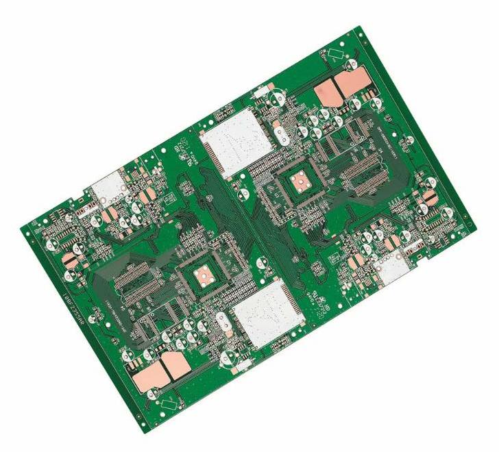
3. The random placement of characters
1) The character cover pad SMD solder tab brings inconvenience to the on-off test of the printed board and the welding of components.
2) The character design is too small, which will make screen printing difficult, and if it is too large, the characters will overlap each other and be difficult to distinguish.
4. The setting of the single-sided pad aperture
1) The single-sided pad is generally not drilled. If the drill hole needs to be marked, the hole diameter should be designed to be zero. If the value is designed so that when the drilling data is generated, the coordinates of the hole appear at this position, the problem occurs.
2) Single-sided pads such as drilled holes should be specially marked.
5. Draw pads with fill blocks
Drawing pads with filling blocks can pass the DRC inspection when designing the circuit, but it is not suitable for processing, so the solder mask data cannot be generated directly with the pads. Device soldering is difficult.
6. The electrical stratum is both a flower pad and a connection
Because the power supply is designed in the form of flower pads, the ground plane is opposite to the image on the actually printed board, and all the connections are isolated lines, which the designer should be very clear about. Here, by the way, be careful when drawing the isolation lines of several groups of power sources or grounds, so as not to leave gaps to short-circuit the two groups of power sources, or to seal the area of the connection (so that one group of power sources is separated).
7. The definition of processing level is not clear
1) The single-panel design is on the TOP layer. If the front and back are not specified, it may be difficult to solder the manufactured board with devices installed.
2) For example, a four-layer board is designed with TOP mid1 and mid2 bottom four layers, but it is not placed in this order during processing, which requires an explanation.
8. Too many padding blocks in the design or padding blocks are filled with extremely thin lines
1) The generated light drawing data is lost, and the light drawing data is incomplete.
2) Since the filled blocks are drawn one by one during the light-drawing data processing, the amount of light-drawing data generated is quite large, which increases the difficulty of data processing.
9. The surface mount device pad is too short
This is for the on-off test. For surface mount devices that are too dense, the distance between the two feet is quite small, and the pads are also quite thin. When installing the test pins, they must be staggered up and down (left and right), such as the pads. If the design is too short, although it will not affect the installation of the device, it will make the test pins in the wrong position.
10. The spacing of large-area grids is too small
The edges between the same lines that make up a large area of grid lines are too small (less than 0.3mm), and in the process of printing the board, after the image transfer process is completed, a lot of broken films are likely to be attached to the board, resulting in broken lines.
11. The distance between the large area of copper foil and the outer frame is too close
The large-area copper foil should be at least 0.2mm away from the outer frame because when milling the shape, if it is milled on the copper foil, it is easy to cause the copper foil to warp and the solder resists to fall off.
12. Uneven graphic design
In the process of pattern plating, the plating layer is uneven, which affects the quality.
13. When the copper area is too large, use grid lines to avoid blistering on the PCB board.