Each layer in a PCB board plays a specific role in determining electrical behavior. Signal plane layers carry power and electrical signals between components, but unless you properly place copper planes in the internal layers, they may not function properly. In addition to the signal layers, your PCB board also needs power and ground planes, and you need to place them in the PCB board stack-up to make sure the new board works properly. So where are the power, ground, and signal layers placed? This is one of the long-standing debates in PCB board design, forcing designers to carefully consider the intended application of their board, the functionality of the components, and the signal tolerances on the board. If you understand the limits of impedance variation, jitter, voltage ripple vs. PDN impedance, and crosstalk rejection, you can determine the correct arrangement of signal and plane layers to place on the board. Bringing your design intent to life requires the right PCB board design toolset. Whether you want to create a simple two-layer board or a high-speed PCB with dozens of layers, PCB board design software needs to be suitable for any application.
When defining a signal plane stack, entry-level designers may be inclined to take things to the extreme. They only need two layers per board or a dedicated layer per small stitch. The correct answer is somewhere in between, depending on the number of nets on the board, the acceptable level of ripple/jitter in the circuit, the presence of mixed signals, etc. In general, if your proof of concept works fine on a breadboard, you can use any layout technique you like on a two-layer board and there's a good chance the board will work. In many cases, you may need to use a grid grounding method for high-speed signals to provide a degree of EMI suppression. For more complex devices that operate at high speeds or high frequencies (or both), you'll need at least four PCB board stack-ups, including a power plane, a ground plane, and two signal planes. When determining the required number of signal plane layers, the first consideration is the number of signal nets and the approximate width and spacing between signals. When you are trying to estimate the number of signal layers required in a stack, there are two basic steps you can take:

Determining the Net Count: A simple net count from the schematic and proposed board dimensions can be used to estimate the number of signal layers required on the board. The number of layers is usually proportional to the score (net*trace width)/(board width). In other words, more nets with wider traces need to make the board larger or need to use more signal layers. You must default to using the experience here to determine the exact number of signal layers required to accommodate all nets in given board size.
Add your plane layers: If you need controlled impedance routing for your signal layers, you now need to place reference layers for each controlled impedance signal layer. If the components are densely packed, a power plane is required below the component layer because there is not enough space on the surface layer to accommodate the power rails. This can result in a double-digit number of surface layers required for high net value HDI boards, but the reference layer will provide shielding and consistent characteristic impedance. Once the correct number of layers for a multi-layer board is determined, you can move on to arranging the number of layers in the PCB board stack-up.
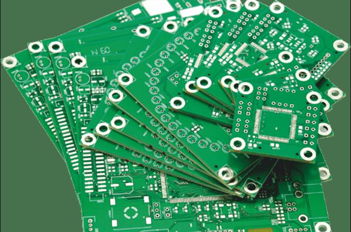
Designing the PCB stack-up
The next step in PCB stack-up design is to arrange each layer to provide trace paths. Your laminates are usually arranged symmetrically around a central core to prevent warping during high-temperature assembly and handling. The placement of plane and signal layers is critical for impedance-controlled routing because you need to use specific equations for different trace placements to ensure impedance is controlled. For rigid-flex stack-up designs, you need to define different regions in the stack-up for rigid-flex regions. The layer stack design tool in Allegro makes this process easy. After the schematic is captured as a blank PCB board layout, layer stacks can be defined, and transitions through the different layers can be defined. You can then proceed to determine the trace size required for controlled impedance routing.
Stripline vs Microstrip and Controlled Impedance
To control the impedance, the traces routed on the inner layer between the two planar layers should be designed using the stripline impedance equation. This equation defines the geometry required for a stripline to have a specific characteristic impedance value. Since there are three different geometric parameters in the equation to determine the impedance, it is easy to first determine the number of layers required, as this will determine the layer thickness for a given board thickness. Copper weights for internal signal plane layers are typically 0.5 or 1 oz./sq.. ft. This uses trace width as a parameter to determine a specific characteristic impedance. The same process applies to microstrip lines on the surface layer. After determining the layer thickness and copper weight, you only need to determine the trace width that defines the characteristic impedance. PCB board design tools include an impedance calculator that can help you size your traces so that they define their characteristic impedance. If you need to use differential pairs, just define the traces in each layer as differential pairs and the impedance calculator will determine the correct spacing between the traces. When routed on the actual board, they can be capacitively or inductively coupled to other traces and conductors. Parasitic capacitance and inductance from nearby conductors can change the trace impedance in the actual layout. To ensure that you have met the impedance target for all layers in the stack, you need an impedance analysis tool to track the impedance throughout the selected signal net. If you see unacceptably large changes in the PCB board layout, you can quickly select traces and adjust the routing to eliminate these impedance changes in the interconnect. where large impedance changes along the trace are marked in red. The spacing between traces in this area should be adjusted to eliminate this impedance variation or bring it within acceptable tolerances. You can define the desired impedance tolerance in the design rules, and the post-layout impedance calculator tool will check the routing against the desired impedance value. In the above discussion, we have only looked at digital signals because they are more demanding than analog systems. What about an all-analog or mixed-signal board? For analog boards, power integrity is much easier, but signal integrity is much more difficult. For mixed-signal boards, you'll need to combine the digital approach shown above with the analog approach described here.
The bandwidth of a digital signal can be extended to a certain high frequency, usually, the corner frequency is taken as the frequency of a binary signal. The corner frequency is about 0.35/(rise time), and for a signal with a rise time of 1ns, the corner frequency is 350MHz. For faster digital signals down to about 20ps, the knee frequency now extends to 17.5GHz. For analog signals, the bandwidth is much narrower, you only need to worry about power plane impedance and insertion/return loss within that bandwidth. This makes power integrity and signal integrity easier. Any loss or high PDN impedance in the signal chain outside this bandwidth is negligible.
Signal isolation
Another option is more aggressive and requires the use of grounded copper powder or through fences to ensure isolation between different parts of the board. If you do the ground pour next to the analog traces, you have just created a coplanar waveguide, which has high isolation and is a common choice for routing high-frequency analog signals. If fences or other high-frequency conductive isolation structures are to be used, the electromagnetic field solver should be used to examine the isolation and determine whether isolation in different signal layers should be selected.
Return plan
Mixing analog and digital signals on the board imposes stringent requirements on tracking ground loop displacement currents and isolation between digital and analog board sections. The layout of the board should ensure that the analog return paths do not cross near the digital components and vice versa. This simply separates digital and analog signals into different layers separated by their respective ground planes. Although this adds cost, it ensures isolation between the different parts. Analog components may also require dedicated analog power strips if they are drawn from AC power. Outside of power electronics, this is a rare case, but conceptually it's easy to handle as long as you can analyze the return path planning. If the analog power section is placed upstream and separated from the digital signal section, a single power plane can be dedicated to both signals. Interference between different power and ground sections can be prevented if the return path is planned correctly. For DC power sections with switching regulators, the switching noise of the DC section needs to be separated from the AC section, just as digital signals need to be separated from analog signals on the PCB board.