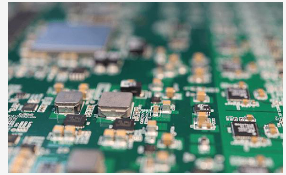
Causes and solutions for PCBA's virtual soldering. Virtual soldering is commonly referred to as cold solder. The surface looks good, but the actual internal connection is not connected, or it is in an intermediate unstable state that may or may not be connected. Some are due to poor soldering or lack of tin, which causes the component pins and solder pads to fail to conduct. Others are caused by oxidation or impurities in the component feet and solder pads, which are indeed not easy to see with the naked eye.
Welding is a common line fault
There are two reasons for false welding:
One is in the PCBA production process, caused by improper production process, the unstable state of the current and the unreasonable;
The other is that after long-term use of electrical appliances, some parts with severe heat generation are very likely to be caused by aging and peeling at the solder joints at the solder feet.
Weak soldering: Generally, it is caused by oxidation or impurities in the solder joints, poor soldering temperature, and improper methods. The essence is that there is an isolation layer between the solder and the pins. They are not completely in contact with each other. Normally, the naked eye cannot see their state. But their electrical characteristics are not connected or poorly connected, which affects the circuit characteristics.
The PCBA components must be stored in moisture-proof, and the in-line electrical appliances can be slightly polished. When soldering, solder paste and flux can be used, preferably a reflow soldering machine. Manual welding requires good technology. As long as the first welding is good, there will be no false welding. After long-term use of electrical appliances, some parts with serious heat generation are prone to aging and peeling of the solder joints at the welding feet.

The method to solve the false welding
1) Judge the approximate fault range based on the occurrence of the fault phenomenon.
2) Appearance observation, focusing on larger components and components with large heat generation.
3) Observe with magnifying glass.
4) Pull the circuit board.
5) Shake the suspicious component by hand and observe whether the solder joints of its pins are loose.
Why is there a false welding?
How to avoid false welding?
The essence of virtual welding is that the temperature of the joint surface of the weld is too low during welding, and the size of the nugget is too small or even to the extent of melting, but it has reached a plastic state. After rolling, it is barely joined together, so it looks good., Actually not fully integrated
The analysis of the causes and steps of false welding can be carried out in the following order:
(1) First check whether the weld joint surface has impurities such as rust, oil, or unevenness, or poor contact. This will increase the contact resistance, reduce the current and reduce the temperature of the welding joint surface.
(2) Check whether the overlap of the weld is normal, and whether the overlap of the drive side is reduced or cracked. The reduction in the amount of overlap will make the combined area of the front and rear steel strips too small, reducing the total force surface and unable to withstand greater tension. In particular, the driving side cracking phenomenon will cause stress concentration, and the cracking will become larger and larger, and finally it will be broken.
(3) Check whether the current setting complies with the process regulations, and whether the current setting does not increase correspondingly when the thickness of the product changes, resulting in insufficient current during welding and poor welding.
If you want to solder well, you must control the PCBA design, and the soldering fire is also very important. The following are the problems and solutions encountered by the long line operation. The key is to understand in practice.
Before welding: basic quality and component control
1 pad design
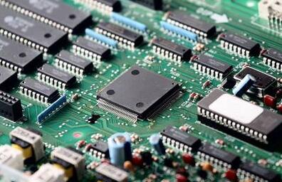
(1) When designing plug-in component pads, the size of the pad should be designed appropriately. If the pad is too large, the spreading area of the solder is larger, and the solder joint formed is not full, while the surface tension of the copper foil of the smaller pad is too small, and the solder joint formed is a non-wetting solder joint. The matching gap between the aperture and the component lead is too large, and it is easy to solder. When the aperture is 0.05-0.2mm wider than the lead, and the diameter of the pad is 2-2.5 times the aperture, it is an ideal welding condition.
(2) When designing SMD component pads, the following points should be considered: In order to remove the "shadow effect" as much as possible, the solder ends or pins of the SMD should be facing the direction of the tin flow to facilitate contact with the tin flow. Reduce false welding and missing welding.
Wave soldering is not suitable for the soldering of fine-pitch QFO, PLCC, BGA and small-pitch SOP devices.
Smaller components should not be arranged after larger components, so as not to prevent the larger components from preventing the tin flow from contacting the pads of the smaller components and causing solder leakage.
2PCB flatness control
Wave soldering has high requirements on the flatness of the printed board. Generally, the warpage is required to be less than 0.5mm, and if it is greater than 0.5mm, it needs to be flattened. In particular, the thickness of some printed boards is only about 1.5mm, and the warpage requirements are even higher, otherwise the welding quality cannot be guaranteed.
3 Properly store printed boards and components
Shorten the storage period as much as possible. During soldering, dust, grease, oxide-free copper foil and component leads are conducive to the formation of qualified solder joints. Therefore, printed boards and components should be stored in a dry and clean environment, and the storage period should be shortened as much as possible . For printed boards that have been placed for a long time, the surface generally needs to be cleaned, which can improve solderability, reduce false soldering and bridging, and remove the surface oxide layer of component pins that have a certain degree of oxidation on the surface.
Production process: quality control of production materials
In wave soldering, the production process materials used are: flux and solder. Discuss separately as follows:
Flux quality control
Flux plays an important role in the control of welding quality. Its functions are:
(1) Remove the oxide on the welding surface;
(2) Prevent re-oxidation of solder and soldering surface during soldering;
(3) Reduce the surface tension of solder;
(4) Contribute to heat transfer to the welding area.
Currently, no-clean fluxes are mostly used in wave soldering. When selecting flux, there are the following requirements:
(1) The melting point is lower than that of solder;
(2) Wetting and spreading speed is faster than melting solder;
(3) Viscosity and specific gravity are smaller than solder;
(4) Stable storage at room temperature, quality control of solder
The tin-lead solder is continuously oxidized at high temperature (250°C), so that the tin content of the tin-lead solder in the tin pot is continuously reduced, deviating from the eutectic point, resulting in poor fluidity, and quality problems such as continuous soldering, virtual soldering, insufficient solder joint strength, etc. . The following methods can be used to solve this problem:
1. Add redox agent to reduce the oxidized SnO to Sn and reduce the generation of tin dross.
2. Continuously remove scum.
3. Add a certain amount of tin before each welding.
4. Use solder containing anti-oxidation phosphorus.
5. Using nitrogen protection, let the nitrogen isolate the solder from the air, instead of ordinary gas, so as to avoid the generation of scum.
3 crest height
The height of the wave crest will change due to the passage of the soldering work time. Appropriate corrections should be made during the soldering process to ensure the ideal height for the soldering wave crest height. The soldering depth is 1/2-1/3 of the PCB thickness. allow. 3.4 Welding temperature
Welding temperature is an important process parameter that affects welding quality. When the soldering temperature is too low, the expansion rate and wetting performance of the solder will become poor, so that the solder pads or the solder ends of the components cannot be fully wetted, resulting in defects such as false soldering, sharpening, and bridging; when the soldering temperature is too high, It accelerates the oxidation of the pads, component pins and solder, and it is easy to produce false soldering. The welding temperature should be controlled at 250+5 degree Celsius.