Frictional electrification and electrification of the human body often occur. PCBA products are inevitably exposed to external or self-contact friction and form a high surface potential during the production, packaging and transportation, and processing, debugging, and testing of the assembled machine. If the operator does not take electrostatic protection measures, the electrostatic potential of the human body can be as high as 1.5~3kV. Therefore, regardless of friction electrification or human body static electricity, it will cause damage to electrostatic sensitive electronic devices. According to the mechanics and discharge effect of static electricity, its electrostatic damage is roughly divided into two categories, which are the adsorption of dust caused by static electricity and the breakdown of sensitive components caused by electrostatic discharge.
Frictional electrification and electrification of the human body often occur in PCBA processing. PCBA products are inevitably exposed to external or self-contact friction and form a high surface during the production, packaging and transportation, and processing, debugging, and testing of the assembled machine. Potential. If the operator does not take electrostatic protection measures, the electrostatic potential of the human body can be as high as 1.5~3kV. Therefore, regardless of friction electrification or human body static electricity, it will cause damage to electrostatic sensitive electronic devices. According to the mechanics and discharge effect of static electricity, its electrostatic damage is roughly divided into two categories, which are the adsorption of dust caused by static electricity and the breakdown of sensitive components caused by electrostatic discharge.

1. Electrostatic adsorption:
SiO2 and high polymer materials are widely used in the manufacturing process of semiconductors and semiconductor devices. Due to their high insulation properties, they tend to accumulate high static electricity during the production process, and are easy to absorb charged particles in the air, resulting in semiconductor interface breakdown, Invalidate. In order to prevent hazards, the manufacture of semiconductors and semiconductor devices must be carried out in a clean room. At the same time, anti-static measures should be taken on the walls, ceilings, floors, operators, and all tools and appliances of the clean room.
2. Electrostatic breakdown and soft breakdown:
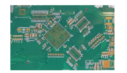
Very large-scale integrated circuits have high integration and high input impedance, and the damage of such devices by static electricity is becoming more and more obvious. In particular, metal oxide semiconductor (MOS) devices have a higher probability of electrostatic breakdown.
Now take the MOS field effect transistor (MOSFET) as an example to illustrate: the aluminum gate of the MOS field effect transistor is covered on the SiO2 film and covers the entire channel. Due to the good insulation performance of the silicon oxide film, the input impedance of the device is as high as 1012Ω or more. When static charges appear on the aluminum grid, the high resistance of the SiO2 film makes it impossible to leak, so it accumulates on the aluminum grid. At this time, the aluminum gate, the SiO2 film and the semiconductor channel are equivalent to a plate capacitor, and the thickness of the SiO2 film is only 103A, its withstand voltage is only 80~100V, and the input capacitance of the field effect tube is only 3pF, even if it is A small amount of charge will also increase the voltage. When the voltage exceeds 100V, it will cause the SiO2 film to be broken down, causing the gate trench to communicate and the device to be damaged. When voltage breakdown occurs, it is often that a network click through occurs at individual points of the SiO2 film under a certain overvoltage. Later, as long as the voltage is lower, a large area of avalanche breakdown will occur, resulting in permanent failure. Sometimes high-voltage static electricity will directly damage the leads inside the chip, causing the IC to permanently fail.
The damage of electrostatic discharge to electrostatic sensitive devices is mainly manifested as:
Hard breakdown. Cause the failure and damage of the entire device at one time.
Soft breakdown. It causes local damage to the device, reduces the technical performance of the device, and leaves hidden dangers that are not easy to be discovered by people, so that the device cannot work normally. The harm caused by soft breakdown is sometimes more dangerous than hard breakdown. In the initial stage of soft breakdown, the performance of the device decreases slightly. During use, over time, it develops into a permanent failure of the component and causes damage to the equipment. .
The mechanism of device failure caused by static electricity is roughly due to the following two reasons: the damage caused by electrostatic voltage, mainly including dielectric breakdown, PCB surface breakdown and gas arc discharge; the damage caused by electrostatic power, mainly including thermal secondary breakdown, Volume breakdown and metal spray melting.
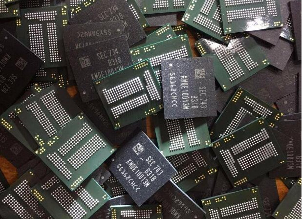
In production, people often refer to electronic devices that are sensitive to electrostatic reactions as Static Sensitive Devices (SSD). This type of electronic devices mainly refers to very large-scale integrated circuits, especially metal oxide film semiconductor (MOS) devices