1. The main inspection contents of manual visual inspection in PCBA processing
SMT chip processing has certain requirements for the workshop environment such as humidity and temperature. At the same time, in order to ensure the quality of electronic components and promote the completion of the processing quantity on schedule, the following requirements are imposed on the workshop environment:
At present, the manual visual inspection in the PCB processing process is mainly through the naked eye or with some relatively simple optical magnification instruments, the manual visual inspection of PCB solder paste printing and solder joints, which is a low investment and effective method, for the process For manufacturers with lower requirements and imperfect equipment and testing equipment, manual visual inspection has played an important role in improving the quality of assembled products.
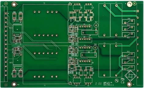
Manual visual inspection includes: manual inspection of printed PCB, manual visual inspection of glue spots, manual visual inspection of solder joints, visual inspection of printed PCB surface quality and so on.
Manual visual inspection is the first thing that needs to be done after solder paste printing, component placement and soldering are completed. The main inspection contents are as follows:

1. Solder paste printing
First check whether the parameter settings of the solder paste printer are correct, the solder paste of the PCB is printed on the pad, whether the height of the solder paste is the same or presents a "trapezoid" shape, and the edges of the solder paste should not be rounded or collapsed into a pile However, it is allowed to have some peak shapes caused by pulling up a small amount of solder paste when the steel plate is detached. If the solder paste is unevenly distributed, it is necessary to check whether the solder paste on the squeegee is insufficient or unevenly distributed. Need to check the printed steel plate and other parameters. Finally, check whether the solder paste is bright after printing under a microscope.
2. Component placement
Before placing the components on the first PCB with solder paste, confirm whether the material rack is properly placed, whether the components are correct, and whether the picking position of the machine is correct before printing. After completing the first PCB, check in detail whether each component is correctly placed and lightly pressed in the center of the solder paste, instead of just being "placed" on top of the solder paste. If you can see a slight depression of the solder paste in the microscope, it means the placement is correct. Whether all the components on the bill of materials (Bill Of Materials, BOM) table are consistent with the components on the PCB, and all components that are sensitive to positive and negative poles, such as diodes, tantalum electrolytic capacitors and ICs, the placement of these components Is the direction correct?
2. Reasons for high cost in PCBA processing
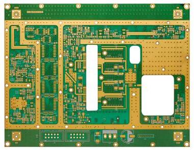
To understand the high cost of PCBA processing, we need to decompose the entire process of packaging labor and materials. PCBA (PCB Assembly) means PCB assembly, so it must include circuit board light board, component welding (smt surface mount /DIP plug-in post welding) these two parts
To understand the high cost of PCBA processing, we need to decompose the entire process of packaging labor and materials. PCBA (PCB Assembly) means PCB assembly, so it must include circuit board light board, component welding (smt surface mount /DIP plug-in post-welding) For these two parts, the current price of light boards on the market is between 350-550, and the prices of components are basically open and transparent in major shopping malls, which can be compared for reference.
Since the main PCB circuit boards and components are not likely to increase prices in the dark, the cost is reflected in the assembly process. The main costs of this link are in the following four aspects:
1. Auxiliary materials: solder paste, tin bar, flux, UV glue, furnace fixture
The quality of solder paste and solder bars is the most important auxiliary material in the entire processing link. Generally, the price of domestic solder paste is 180~260/bottle, and the imported solder paste may be 320~480/bottle, so on the same soldering area, The price of imported solder paste is much higher, but the difference in soldering quality is very obvious.
The price of SMD processing varies according to the number of points and packaging. Large quantity and high price are the consensus of the industry. The larger the component package size, the easier it is to mount, and the corresponding poor quality will be reduced. Therefore, there is more room for communication on the price.
3. Welding hours after DIP plug-in
Because the plug-in material link involves special-shaped parts and material molding, this link requires a lot of manual participation, because there is no reference to the production capacity of machinery and equipment, this link is the link that is the most difficult to control. At the same time, labor costs remain high at present, and the cost of this link is generally high.
4. Assembly test: test fixture, test equipment, test man-hour
The test fixture currently ranges from tens to hundreds of dollars depending on the difficulty of the test, and the test of communication equipment requires the assistance of optical fiber, ICT and other test equipment. The corresponding labor and equipment loss need to be taken into account, but it will not be very high. Some companies even test it for free.