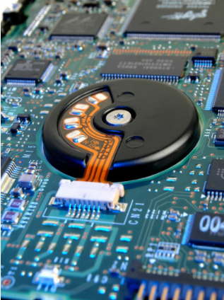
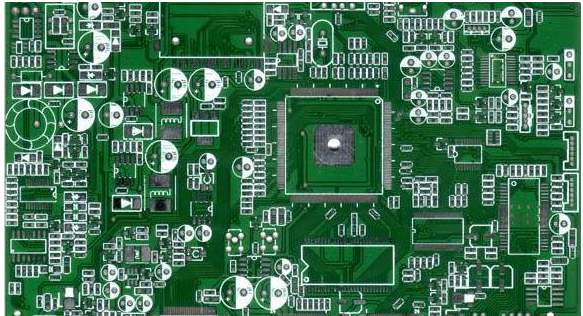
In some applications, conformal coating is necessary, SMT chip processing plant to protect the components on the PCB from physical shock and moisture corrosion in the harsh environment that may cause product failure.
If the conformal coating is not applied properly, the long-term reliability of SMT products may be affected. For example, coating defects in the manufacturing process of automotive electronic modules can threaten the safety and security of passengers. Even in today's era of highly automated manufacturing processes, many companies still manually inspect conformal coatings. In this case, human error may occur depending on the operator’s proficiency and fatigue factors. Reducing such human error and improving the quality and repeatability of the inspection process are the functions of the automatic conformal coating inspection machine.
The key to defect detection of conformal coatings is the illuminance of the coating. This is achieved by adding a tracer material to the coating, which emits light when exposed to an ultraviolet light source. PARMI's PCI 100 lighting system (1) uses UV LED lighting to obtain inspection images for conformal coating and bubble detection (2) uses white light LED lighting for teaching and fiducial mark recognition.

PARMI uses a very innovative synchronous image acquisition technology to perform a single scan from UV LED and white light LED, so the inspection time is very fast. After scanning the sample-coated PCB, the SMT chip processing factory only needs to click the magic wand button, and the programmer can define the coated and non-coated (reserved) areas on the PCB. PARMI's PCI 100 can check the following properties of coated PCBs: coating presence, coating missing (reserved), overspray/contamination, air bubbles, and the coating thickness can be measured at the designated location.
As mobile devices and wearable devices become smaller and thinner, the coating thickness must be strictly controlled. The coating must be thick enough to protect the components, and thin enough to have portability and minimize the consumption of coating materials. In order to meet the coating thickness standard, you can choose to add PARMI's CTS I (coating thickness sensor) to the PCI 100 machine. The laser module in the PCI 100 sensor head first finds the height of the measurement target on the PCB, and then adjusts the Z axis to a precise focal length before the thickness measurement, which improves the measurement reliability of the thickness sensor. coating.
PARMI's PCI 100 DSI (double-sided inspection) can inspect the top and bottom of the PCB in one continuous operation by flipping the PCB inside the machine. It maximizes production efficiency by minimizing unnecessary processes and shorter cycle times. SMT placement processing plants also minimize the required footprint by eliminating the need for external board flippers.
The above is the introduction of the perfect optical inspection of the conformal coating of the SMT chip processing plant