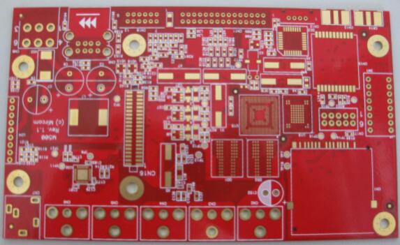
PCB circuit board manufacturers often need to plate rare metals on board edge connectors, board edge protruding contacts or gold fingers to provide lower contact resistance and higher wear resistance. This technology is called finger row plating or protruding parts. plating. Gold is often plated on the protruding contacts of the board edge connector with the inner plating layer of nickel, and the gold fingers or the protruding parts of the board edge are manually or automatically plated. At present, the gold plating on the contact plug or gold finger has been rhodium-plated or lead-plated Replaced.
The first type, finger row electroplating
It is often required to plate rare metals on board edge connectors, board edge protruding contacts or gold fingers to provide lower contact resistance and higher wear resistance. This technique is called finger row plating or prominent partial plating. Gold is often plated on the protruding contacts of the board edge connector with the inner plating layer of nickel. The gold finger or the protruding part of the board edge is manually or automatically electroplated. At present, the gold plating on the contact plug or gold finger has been plated or leaded., Replaced by plated buttons. The process is as follows:
1) Strip the coating to remove the tin or tin-lead coating on the protruding contacts
2) Rinse with washing water
3) Scrubbing with abrasives
4) The activation is diffused in 10% sulfuric acid
5) The thickness of nickel plating on the protruding contacts is 4 -5μm
6) Clean and demineralize water
7) Disposal of gold soaking solution
8) Gold plated
9) Cleaning
10) Drying

The second type, through-hole plating
There are many ways to build a plating layer that meets the requirements on the hole wall of the substrate drilled hole. This is called hole wall activation in industrial applications. The printed circuit commercial production process requires multiple intermediate storage tanks. The tank has its own control and maintenance requirements. Through-hole plating is a necessary follow-up manufacturing process of the drilling manufacturing process. When the drill bit drills through the copper foil and the substrate underneath, the heat generated condenses the insulating synthetic resin that constitutes most of the substrate matrix, and the condensed resin and other drilling debris It is piled up around the hole and coated on the newly exposed hole wall in the copper foil. In fact, this is harmful to the appearance of subsequent electroplating. The condensed resin will also leave a layer of hot shaft on the wall of the substrate hole. It exhibits poor adhesion to most activators. This requires the development of a similar technology for stain removal and etch back chemistry.
A more suitable method for prototyping printed circuit boards is to use a specially designed low-viscosity ink to form a high-adhesion, high-conductivity film on the inner wall of each through hole. In this way, there is no need to use multiple chemical treatment processes, only one application step, and then the thermal curing is stopped, a continuous film can be formed on the inner side of all the hole walls, and it can be directly electroplated without further treatment. This ink is a resin-based substance that has a very strong adhesion and can be easily bonded to the walls of most thermally polished holes, thus eliminating the etch-back step.
The third type, reel linkage type selective plating
The pins and pins of electronic components, such as connectors, integrated circuits, transistors and flexible printed circuits, use selective plating to achieve good contact resistance and corrosion resistance. This plating method can be manual or automatic. It is very expensive to select plating for each pin individually, so batch welding must be used. Usually, the two ends of the metal foil that is rolled to the required thickness are stopped for punching, and the cleaning is stopped by chemical or mechanical means, and then selectively used such as nickel, gold, silver, rhodium, button or tin-nickel alloy, copper-nickel alloy, Nickel-lead alloy, etc. stop continuous electroplating. When choosing the electroplating method of plating, first coat a layer of resist film on the part of the metal copper foil board that does not need to be electroplated, and stop electroplating only on the selected part of the copper foil.
The fourth type, brush plating
Another method of selective plating is called "brush plating". It is an electric accumulation technology, and not all parts are immersed in the electrolyte during the electroplating process. In this kind of electroplating technology, electroplating is only stopped in a limited area, and there is no effect on other parts. Usually, rare metals are plated on selected parts of the printed circuit board, such as areas such as board edge connectors. Brush plating is more used when repairing discarded PCB circuit boards in electronic assembly workshops. Wrap a special anode (anode with inactive chemical reaction, such as graphite) in an absorbent material (cotton swab), and use it to bring the electroplating solution to the center where the electroplating needs to be stopped.