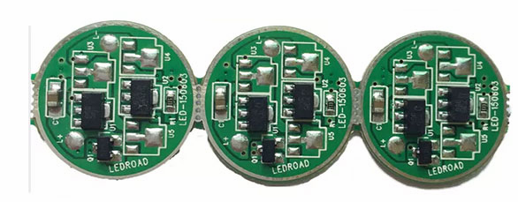
The silk screen layer of the PCB circuit board is the text layer. Its function is to facilitate the installation and maintenance of the circuit. The required logo patterns and text codes are printed on the upper and lower surfaces of the PCB circuit board, such as component numbers and nominal values. Component outline shape and manufacturer logo, production date, etc. So what are the specifications and requirements for the silk screen of the PCB circuit board, the following are for reference:
1. All components, mounting holes, and positioning holes have corresponding silk-screen marks. In order to facilitate the installation of PCB circuit boards, all components, mounting holes, and positioning holes have corresponding silk-screen marks. The mounting holes on the PCB circuit board are used for silk-screening. H1, H2...Hn are identified.
2. Silk-screen characters follow the principle of left to right and bottom-up. Silk-screen characters should follow the principle of left-to-right and bottom-up as far as possible. For devices with polarities such as electrolytic capacitors and diodes, try to keep them in each functional unit. The direction is the same.
3. There is no silk screen on the device pad and the tin track that needs to be tinned, and the device position number should not be blocked by the device after installation. (The density is high, except for those that do not need to be silk-screened on the PCB circuit board)

In order to ensure the soldering reliability of the device, it is required that there is no silk screen on the device pad; in order to ensure the continuity of the tin enamel, it is required to have no silk print on the enamel tin; in order to facilitate the device insertion and maintenance, the device location number should not be The device is blocked after installation; the silk screen should not be pressed on the via hole and the pad, so as to avoid the loss of part of the silk screen when the solder mask window is opened, which will affect the training. The silk screen spacing is greater than 5mil.
4. The polarity of the components with polarity is clearly indicated on the silk screen, and the polarity direction mark is easy to identify.
5. The direction of the directional connector is clearly indicated on the silk screen.
6. The position of the printed board information such as the name, date, and version number of the PCB circuit board should be clear. The PCB circuit board file should have the board name, date, version number and other finished board information silkscreen, the location is clear and eye-catching.
7. The complete manufacturer's relevant information and anti-static signs should be on the PCB circuit board.
8. The number of light drawing files of the PCB circuit board is correct, and each layer should have the correct output, and there should be a complete output of the number of layers.
9. The identifier of the device on the PCB circuit board must be consistent with the identification symbol in the BOM list.
ipcb specializes in the production of IC packaging substrates, BGA substrates, LGA substrates, CSP packaging substrates, PGA substrates, MCM substrates, PKG substrates, QOFP substrates, chip packaging substrates