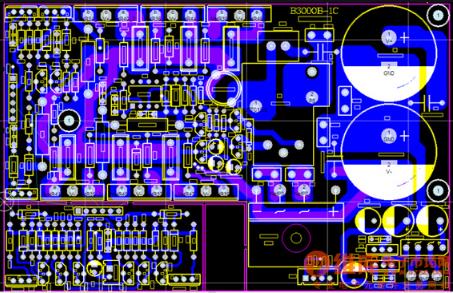
In the process of designing the PCB circuit board, seemingly simple vias, if you do not leave a sound, it is likely to bring great negative effects to the circuit board. Today, I will tell you how to reduce the adverse effects of the parasitic effects of the vias in the via design of the PCB circuit board:
The pins of the power supply and the ground should be drilled nearby, and the lead between the via and the pin should be as short as possible, because they will increase the inductance. At the same time, the power and ground leads should be as thick as possible to reduce impedance.
2. Try not to change the layers of the signal traces on the PCB circuit board, that is to say, trynot to use unnecessary vias.
3. The use of a thinner PCB circuit board is beneficial to reduce the two parasitic parameters of the via.
4. Considering the cost and signal quality, choose a reasonable size of the via hole. For example, for the 6-10 layer memory module PCB circuit board design, it is better to use 10/20Mil (drilled/pad) vias. For some high-density small-size boards, you can also try to use 8/18Mil Of vias. Under current technical conditions, it is difficult to use smaller vias. For power or ground vias, you can consider using a larger size to reduce impedance.
5. Place some grounded vias near the vias of the signal layer to provide the nearest loop for the signal. It is even possible to place a large number of redundant ground vias on the PCB circuit board. Of course, the design needs to be flexible.

The via model discussed earlier is the case where there are pads on each layer. Sometimes, we can reduce or even remove the pads of some layers. Especially when the density of vias is very high, it may lead to the formation of a broken groove in the copper layer to isolate the loop. To solve this problem, in addition to moving the position of the via, we can also consider placing the via on the copper layer. The pad size is reduced.
6. Avoid entering the minefield when making circuit board PCB proofing
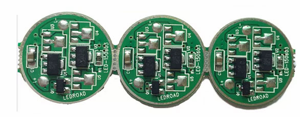
PCB proofing makes the circuit miniaturized and intuitive, and plays an important role in the mass production of fixed circuits and the optimization of electrical layout.
Dual-disk is an extension of single-disk. When single-layer wiring cannot meet the needs of electronic products, dual-disk is used. Both sides are covered and wired, and the wiring between the two layers can pass through holes to form the required network connection.
7. Avoid entering the minefield when doing PCB proofing, pay attention to appearance
The quality of PCB is evaluated from the aspects of PCB welding, light, color, board size and thickness. Therefore, PCB multi-layer PCB proofing manufacturers should start from these aspects and carefully complete the appearance requirements of PCB proofing.
8. Pay attention to staffing
In the proofing process, each process requires special technical personnel to supervise and control, and is responsible for inspecting the production circuit boards of each process. At the same time, after the product is completed, special personnel are required to conduct a comprehensive inspection or sampling inspection, in order to ensure the PCB Proofing quality of multi-layer circuit boards.
9. Attention should be paid to material selection
At present, one side and a half glass plate is a good quality raw material, with good strength, both sides are green, and copper-coated without peculiar smell. Compared with other plates, the cost is slightly higher. If the price of HB plate is favorable, there will be phenomena such as line change and breakage, and the quality of proofing will be rougher.