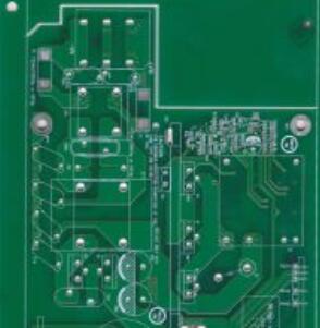
With the rapid development of the PCB industry, PCB is gradually moving towards the direction of high-precision thin lines, small apertures, and high aspect ratios (6:1-10:1). The hole copper requirements are 20-25Um, and the DF line spacing is less than 4MIl. Generally, PCB companies have problems with electroplating interlayers. The following editor will talk about the causes of electroplating interlayer film in the multi-layer PCB proofing process and how to improve the treatment.
Causes of electroplating interlayer film during multi-layer PCB proofing
1. The pattern of the board is not uniformly distributed. During the pattern electroplating process, due to the high potential of several isolated lines, the plating layer exceeds the film thickness, forming a sandwich film and causing a short circuit.
2. The anti-plating film layer is too thin. During electroplating, the plating layer exceeds the film thickness, forming a PCB sandwich film. In particular, the smaller the line spacing, the easier it is to cause the film short circuit.
Method for improving electroplating interlayer film in multi-layer PCB proofing process
Increase the thickness of the anti-plating layer: choose a dry film with a suitable thickness. If it is a wet film, you can use a low-mesh screen printing, or increase the film thickness by printing the wet film twice.
2. The plate pattern is unevenly distributed, which can appropriately reduce the current density (1.0~1.5A) for electroplating. In daily production, we want to ensure the output, so we usually control the electroplating time as short as possible, so the current density used is generally between 1.7 and 2.4A.
In this way, the current density obtained in the isolated area will be 1.5 to 3.0 times that of the normal area, which often results in the coating height of the isolated area with a small distance exceeding the film thickness by a lot. The phenomenon that the edge clamps the anti-coating film, which causes the film short circuit, and at the same time makes the solder mask on the circuit thinner.

At the same time, as the functions of current electronic products are becoming more and more complex, the power consumption is increasing; the heat generated by the system is also increasing, and the integration density of the PCB is getting higher and higher. According to relevant data, the area of the PCB board has been reduced by half, while the components integrated on the board have increased by 3.5 times, and the integration density of the entire PCB board has increased by 7 times.
What are the requirements for the size of the vias in the production of PCB boards
PCB boards and systems are moving towards higher density, faster speed, and greater heat generation. In addition, the problems caused by the overheating of the circuit board are getting more and more attention, and thermal simulation will become an indispensable step in the electronic PCB design process. The traditional thermal simulation test mainly focuses on the selection of the size of the PCB via hole in the product. Usually the R outer diameter-r inner diameter >=8mil (0.2mm)
It is generally recommended that the outer diameter is 1MM, the inner diameter is 0.3-0.5MM, and the more dense lines, the outer diameter should be 0.6MM, and the inner diameter should be 0.4-0.2MM.
The outer diameter can be made larger for the large current, and the hole can be made smaller. However, PCB manufacturers generally recommend using 0.5MM inner diameter, because they are not easy to break with a 0.5 drill bit. The drill bit below 0.5mm is easy to break.
However, as electronic products become lighter, thinner, shorter, and smaller, many electronic products have been compressing design parameters in order to reduce the size of the board. As a result, there is no place to place 0.3mm vias, and they can only be designed to be 0.15-0.25. For holes of about mm, it is more difficult to make such holes. If it is not necessary, try not to design holes of this size.
Generally speaking, the via hole is designed to have a diameter of 0.3mm, and most factories can meet the production requirements. If it is set below 0.3mm, many factories cannot produce due to the limitation of production equipment. Even if some factories can produce, the scrap will be very large. The cost will increase.