What are the PCB proofing processing procedures?
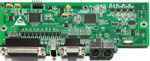
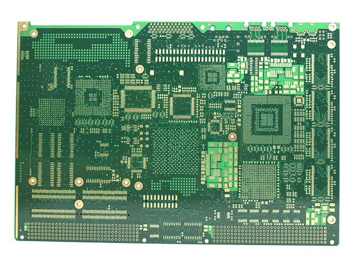
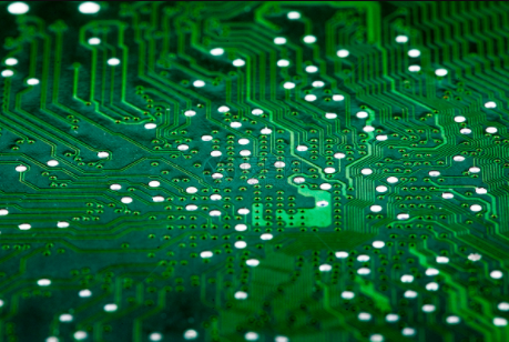
In electronic equipment, the printed circuit board is a key part. It is equipped with other electronic components and connected to the circuit to provide a stable circuit working environment. So, what are the PCB proofing processing procedures? Take the six-layer board as an example, let’s take a look:
[Inner circuit] The copper foil substrate is first cut into a size suitable for processing and production. Before the substrate is laminated, it is usually necessary to properly roughen the copper foil on the surface of the board, and then attach the dry film photoresist to it at an appropriate temperature and pressure; then, the substrate is sent to the UV exposure machine for exposure, and the The circuit image on the film is transferred to the dry film photoresist on the board. After tearing off the protective film, first use sodium carbonate aqueous solution to develop and remove the unlit area on the film surface, and then use the hydrogen peroxide mixed solution to corrode and remove the exposed copper foil to form a circuit. Finally, the dry film photoresist is washed off with a lightly oxidized sodium water solution.
【Pressing】Before pressing, the inner layer board is black (oxidized) treated to passivate the copper surface to increase insulation; and the copper surface of the inner layer circuit is roughened to produce good adhesion performance. When laminating, first riveting the inner circuit boards of six layers (including) with a riveting machine; then use a tray to neatly stack them between the mirror steel plates, and send them to the vacuum laminating machine for appropriate temperature and pressure Make the film harden and bond. The laminated circuit board uses the X-ray automatic positioning drilling machine to drill the target hole as the reference hole; and properly cut the edge of the board to facilitate subsequent processing.
[Drilling] The circuit board is drilled with a CNC drilling machine to drill the through holes of the interlayer circuit and the fixing holes of the welding parts.
[Plated through holes] After forming the interlayer vias, a metal copper layer needs to be laid on it to complete the interlayer circuit conduction. First, use heavy brushing and high-pressure washing to clean the hair on the hole and the powder in the hole, and soak the tin on the clean hole wall.

[Primary copper] Immerse the circuit board in a chemical copper solution, and deposit the copper ions in the solution on the hole wall to form a through-hole circuit; then add the copper layer in the via hole by electroplating with a copper sulfate bath Thick enough for subsequent processing.
[Outer circuit secondary copper] The production of the circuit transfer is the same as the inner circuit, but the circuit etching is divided into two ways: positive and negative. The negative film is made in the same way as the inner circuit. After the development, the copper is directly etched and the film is removed. The positive film method is to add secondary copper and tin-lead plating after development. After removing the film, the exposed copper foil is corroded and removed with a mixed solution of ammonia and copper chloride to form a circuit; finally, tin and lead stripping solution is used to remove the tin The lead layer is stripped.
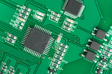
[Solder Resistant Ink Text Printing] Print the text, trademark or part number required by the customer on the board surface by screen printing, and then heat the text (or ultraviolet radiation) to harden the text lacquer ink.
[Contact processing] The solder mask green paint covers most of the copper surface of the circuit, and only the terminal contacts for part welding, electrical testing and circuit board insertion are exposed. This end point needs to be added with a suitable protective layer to avoid oxides during long-term use, which will affect the stability of the circuit.
[Forming and cutting] The circuit board is cut into the external size required by the customer with a CNC molding machine; finally, the powder and the surface ionic contaminants on the circuit board are cleaned.
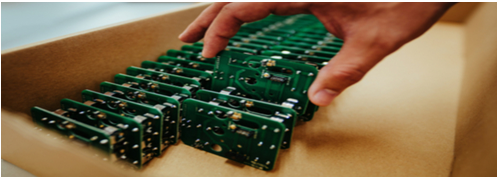
[Check board packaging] Commonly used packaging PE film packaging, heat shrinkable film packaging, vacuum packaging, etc.
The above is the PCB proofing process that the engineer explained in detail for you. I hope it will be helpful to you.