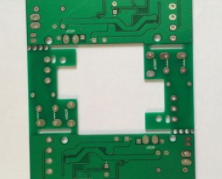
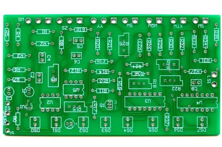
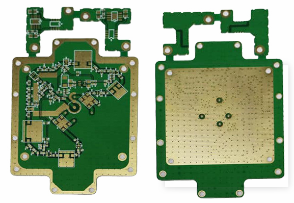
From a technical point of view, multi-layer PCB has many advantages in design. These advantages of multilayer printed circuit boards include:
1. Small size: One of the most prominent and popular advantages of using multilayer printed circuit boards is their size. Due to its layered design, the multilayer PCB itself is smaller than other PCBs with similar functions. This has brought huge benefits to modern electronic products, because the current trend is to focus on smaller, more compact, and more powerful gadgets, such as smart phones, laptops, tablets, and wearable devices.
2. Lightweight structure: Use a smaller PCB and lighter weight, especially because multiple connectors required for interconnection between single-layer and double-layer PCB s are eliminated, which is conducive to multi-layer design. This again benefits modern electronic products, which are more mobile.

3. High quality: Since manufacturing multi-layer PCBs requires a lot of work and planning, these types of PCBs are usually better than single-layer and double-layer PCBs. So they are also more reliable.
4. Increase durability: Multi-layer PCBs are usually durable due to their properties. These multi-layer PCBs must not only bear their own weight, but also be able to handle the heat and pressure of bonding together. In addition to these factors, multilayer PCBs use multiple insulating layers between circuit layers, combined with prepreg adhesives and protective materials.
5. Enhance flexibility: Although it is not suitable for all multi-layer PCB components, some do use flexible structure technology, thus forming a flexible multi-layer PCB. For applications where slight bends and bends may occur on a semi-regular basis, this may be an ideal feature. Similarly, this does not apply to all multilayer PCBs. The more layers added to a flexible PCB, the less flexible the PCB.
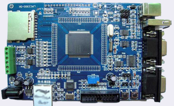
6. More powerful functions: Multi-layer PCB is a very high-density component, which combines multiple layers into a PCB. These close distances make the circuit board more connected, and its inherent electrical properties allow it to achieve greater capacity and speed, albeit in a smaller size.
7. Single connection point: Multi-layer PCB design is used as a single unit, rather than in series with other PCB components. Therefore, they have a single connection point instead of the multiple connection points required to use multiple single-layer PCBs. This proves to be beneficial in the design of electronic products as they only need to include a single connection point in the final product. This is particularly useful for small electronic products and accessories designed to minimize size and weight.
These advantages make multilayer PCBs very useful in various applications, especially mobile devices and high-function electronic devices. On the contrary, as many industries turn to mobile solutions, multilayer PCBs have a place in more and more industry-specific applications.