First, throw up the question: Where should the coil go?
Switching regulators for voltage conversion use inductance to temporarily store energy. These inductors are usually very large in size and must be located in the printed circuit board (PCB) layout of the switching regulator. This task is not difficult because the current flowing through the inductor can change, but not instantaneously. Change can only be continuous and is usually relatively slow.
Switching regulators switch current back and forth between two different paths. This switching is very fast, depending on the duration of the switching edge. The lines through which switching current flows are called thermal circuits or ALTERNATING current paths, which conduct current in one switching state and not in the other switching state. In PCB layouts, the thermal loop area should be small and the path short to minimize the parasitic inductance in these routes. Parasitic wire inductance can produce unwanted voltage imbalance and lead to electromagnetic interference (EMI).

Therefore, it can be assumed that the placement of the inductor is not important. It is correct to have the inductor outside the hot loop--so in this case, placement is of secondary importance. However, there are some rules that should be followed. Sensitive control wiring shall not be laid under the inductor (not on or below the PCB surface), in the inner layer or on the back of the PCB. Under the influence of current flow, the coil creates a magnetic field, which can affect weak signals in the signal path. In switching regulators, a critical signal path is the feedback path, which connects the output voltage to the switching regulator IC or resistance divider.
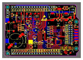
It should also be noted that actual coils have both capacitive and inductive effects. The windings are directly connected to the switch node of the step-down switch regulator. As a result, the voltage in the coil changes as strongly and rapidly as the voltage at the switching node. Because the switching time in the circuit is very short and the input voltage is very high, there is considerable coupling effect on the other paths on the PCB. Therefore, sensitive wiring should be kept away from the coil. As can be seen from the figure, the yellow feedback path is at a certain distance from the coil L1. It is located in the inner layer of the PCB.
Some circuit designers don't even want any copper layers in the PCB under the coil. For example, they provide a notch below the inductor, even in a grounded plane layer. The goal is to prevent eddy currents from forming in the ground plane below the coil due to the coil's magnetic field. There is nothing wrong with this approach, but it is also argued that the grounding plane should remain consistent and should not be interrupted:
The grounding plane used for shielding is effective without interruption.
The more copper a PCB has, the better it dissipates heat.
Even if eddies are generated, these currents flow only locally, cause only small losses, and hardly affect the function of the ground plane.
Therefore, it is agreed that the grounding plane layer, even below the coil, should remain intact.