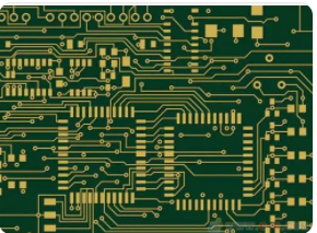
Via is one of the important components of multi-layer PCB. The cost of drilling usually accounts for 30% to 40% of the cost of PCB manufacturing. Simply put, every hole on the PCB can be called a via.
From the point of view of function, vias can be divided into two categories:
Used as electrical connection between layers;
Used for fixing or positioning of devices;
In terms of process, these vias are generally divided into three categories:
Blind via
Buried via
Through via
Blind hole
It is located on the top and bottom surfaces of the printed circuit board and has a certain depth, which is used for the connection of the surface circuit and the underlying inner circuit. The depth of the hole usually does not exceed a certain ratio (aperture).
Buried hole
It refers to the connection hole located in the inner layer of the printed circuit board, which does not extend to the surface of the circuit board. The above-mentioned two types of holes are located in the inner layer of the circuit board, and are completed by a through-hole forming process before lamination, and several inner layers may be overlapped during the formation of the via.
Through hole
This kind of hole penetrates the entire circuit board and can be used for internal interconnection or as a component installation positioning hole. Because the through hole is easier to implement in the process and the cost is lower, most of the printed circuit boards use it instead of the other two types of via holes. The following via holes, unless otherwise specified, are considered as via holes.
From a design point of view, a via is mainly composed of two parts:
Drill hole
Pad area around the drill hole
The size of these two parts determines the size of the via. Obviously, in high-speed, high-density PCB design, designers always hope that the smaller the via hole is, the better, so that more wiring space can be left on the board. In addition, the smaller the via hole, the greater its parasitic capacitance. Small, more suitable for high-speed circuits. However, the reduction in hole size also brings about an increase in cost, and the size of vias cannot be reduced indefinitely. It is limited by process technologies such as drilling and plating: the smaller the hole, the more drilling The longer the hole takes, the easier it is to deviate from the center position; and when the depth of the hole exceeds 6 times the diameter of the drilled hole, it cannot be guaranteed that the hole wall can be uniformly plated with copper. For example, the thickness (through hole depth) of a normal 6-layer PCB board is about 50Mil, so the smallest drill hole diameter that PCB manufacturers can provide can only reach 8Mil. With the development of laser drilling technology, the size of the hole can be smaller and smaller. Generally, a via with a diameter less than or equal to 6Mils is called a micro-hole. Microvias are often used in HDI (High Density Interconnect Structure) design. Microvia technology allows vias to be directly punched on the pad (Via-in-pad), which greatly improves circuit performance and saves wiring space.
The effect of vias on signal transmission: parasitic capacitance and parasitic inductance
Vias appear as breakpoints with discontinuous impedance on the transmission line, which will cause signal reflections. Generally, the equivalent impedance of the via is about 12% lower than that of the transmission line. For example, the impedance of a 50 ohm transmission line will decrease by 6 ohms when passing through the via (specifically, it is related to the size and thickness of the via, not an absolute reduction). However, the reflection caused by the discontinuous impedance of the via is actually very small. The reflection coefficient is only: (44-50)/(44+50)=0.06. The problems caused by the via are more concentrated on the parasitic capacitance and inductance. Impact.

The via itself has parasitic stray capacitance. If it is known that the diameter of the solder mask on the ground layer of the via is D2, the diameter of the via pad is D1, the thickness of the PCB board is T, and the dielectric constant of the board substrate Is ε, then the parasitic capacitance of the via is approximately as follows:
C=1.41*ε*T*D1/(D2-D1)
The main effect of the parasitic capacitance of the via on the circuit is to extend the rise time of the signal and reduce the speed of the circuit. For example, for a PCB with a thickness of 50Mil, if the diameter of the via pad is 20Mil (the diameter of the hole is 10Mils), and the diameter of the solder mask is 40Mil, then we can approximate the size of the via using the above formula The parasitic capacitance is roughly:
C=1.41*4.4*0.050*0.020/(0.040-0.020) =0.31pF
The amount of change in rise time caused by this part of the capacitance is roughly:
T10-90 =2.2C(Z0/2) =2.2*0.31*(50/2) =17.05ps
From these values, it can be seen that although the effect of the rise delay caused by the parasitic capacitance of a single via is not very obvious, if the via is used multiple times in the trace to switch between layers, multiple vias will be used., The design must be carefully considered. In the actual design, the parasitic capacitance can be reduced by increasing the distance between the via and the copper area (Anti-pad) or reducing the diameter of the pad.
Parasitic capacitances exist in vias as well as parasitic inductances. In the design of high-speed digital circuits, the harm caused by the parasitic inductances of vias is often greater than the impact of parasitic capacitances. Its parasitic series inductance will weaken the contribution of the bypass capacitor and weaken the filtering effect of the entire power system. We can use the following empirical formula to simply calculate the parasitic inductance of a via:
L=5.08*h*[ln(4*h/d)+1]
Among them: L refers to the inductance of the via hole h is the length of the via hole d is the diameter of the center hole.
It can be seen from the formula that the diameter of the via has a small influence on the inductance, and the length of the via has the greatest influence on the inductance. Still using the above example, the inductance of the via can be calculated as:
L=5.08*0.050*[ln(4x0.050/0.010)+1] =1.015nH
If the rise time of the signal is 1ns, then its equivalent impedance is:
XL = 2πL/T=6.37Ω
Such impedance can no longer be ignored when high-frequency currents pass. Special attention should be paid to the fact that the bypass capacitor needs to pass through two vias when connecting the power plane and the ground plane, so that the parasitic inductance of the vias will increase exponentially.
How to use vias
Through the above analysis of the parasitic characteristics of vias, we can see that in high-speed PCB design, seemingly simple vias often bring great negative effects to circuit design. In order to reduce the adverse effects caused by the parasitic effects of the vias, the design can be done as much as possible: considering the cost and signal quality, select a reasonable size of the via. If necessary, consider using vias of different sizes. For example, for the 6-10 layer memory module PCB design:
It is better to use 10/20Mil (drilled/pad) vias. For some high-density small-size boards, you can also try to use 8/18Mil vias. Under current technical conditions, it is difficult to use smaller vias. For power or ground vias, you can consider using a larger size to reduce impedance. For signal traces, smaller vias can be used. Of course, as the size of the via decreases, the corresponding cost will increase.
The two formulas discussed above can be concluded that the use of a thinner PCB is beneficial to reduce the two parasitic parameters of the via.
Try not to change the layers of the signal traces on the PCB board, that is, try not to use unnecessary vias.
The pins of the power supply and the ground should be punched nearby, and the leads between the vias and the pins should be as short as possible, because they will increase the inductance. At the same time, the power and ground leads should be as thick as possible to reduce impedance. Consider drilling multiple vias in parallel to reduce the equivalent inductance.
Place some grounded vias near the vias of the signal change layer to provide the nearest return path for the signal. You can even place some redundant ground vias on the PCB.
For high-density high-speed PCB boards, you can consider using micro vias.
Of course, the design needs to be flexible. The via model discussed earlier is the case where there are pads on each layer. Sometimes, we can reduce or even remove the pads of some layers. Especially when the density of vias is very high, it may lead to the formation of a break groove that separates the loop in the copper layer. To solve this problem, in addition to moving the position of the via, we can also consider placing the via on the copper layer. The pad size is reduced.