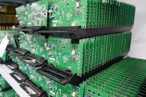
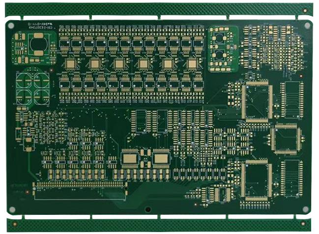
Smaller PCBs, including rigid-flex circuits, require one of three methods for chip placement, depending on the application. Technology that has been the only field of semiconductor manufacturing for many years has now migrated to today's printed circuit board (PCB) manufacturing processes and processes.
These are not the old, traditional PCBs that we grew up with; on the contrary, they are a new type of circuit boards, mainly small rigid circuits and flexible circuits, or a combination of the two, called rigid-flexible combinations. More and more small electronic products, such as wearable devices, portable devices and Internet of Things devices, are based on these updated micro circuit boards.
In 2019 and in the future, as today's advanced electronic products are shrinking the PCB space, microelectronics will play a vital role. One reason for the shrinking circuit board size is that components are also shrinking in size and becoming more and more refined, and it is becoming more and more difficult to assemble, inspect, and test products.
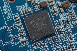
For example, many of these smaller PCBs cannot pass through traditional PCB assembly and manufacturing lines. More and more such circuit boards must go through specialized microelectronic packaging, including wire bonding and chip connection.
Chip connection is a relatively new area of small PCB manufacturing. In short, it is the process of connecting a chip or die to its package, substrate, or rigid, flexible, or rigid-flex circuit. In fact, it may even involve connecting one chip to another.
The chip mounting method to be used depends on the thermal conductivity and heat dissipation. Therefore, before the chip connection process, each chip must undergo careful thermal conductivity inspection and analysis to determine the amount of heat it will emit.
Chips are usually found on tape, in wafers, or in waffle trays. The waffle tray or chipset has many sliced chips (Figure 1).

Figure 1: Waffle Pack with chip (Source: NexLogic Technologies)
When the target chip is picked up from the waffle tray or wafer package by a small vacuum suction tool, the chip connection process begins (Figure 2).
Figure 2: Vacuum suction tool for picking up chips (Source: NexLogic Technologies)
After the die is released by the vacuum, it is precisely aligned with the substrate or PCB, and then permanently connected using one of three methods. The epoxy and solder used for the patch can be non-conductive or conductive. During chip mounting, there should be perfect contact between the chip/chip and the substrate/PCB; in addition, there should be no gaps.
In addition, the adhesive that connects the chip to the substrate must be very precise. This process is very sensitive; in addition to picking up the chip, it must also be placed on the substrate without damaging or destroying it. The die bond created should be able to withstand extremely high temperature ranges without any productivity loss, any performance loss, and any significant degradation.
Typical chip connection methods are epoxy bonding, eutectic and solder connection. The epoxy bonding process may involve silver epoxy glass or polyimide-based materials. This epoxy is dispensed using a very fine dispenser that dispenses the quantity very accurately, with tolerances in microns. In this case, the substrate needs to be heated to a temperature from room temperature to 200°C, depending on the type of epoxy used. This temperature allows the epoxy resin to cure properly so that it adheres to the substrate, thereby accurately forming a joint between the substrate and the chip.
When epoxy is dispensed, it covers the area where the chip connection needs to be made and creates a rounded corner on the edge of the bond. If too much epoxy is dispensed, it will cause contamination and dislocation. Coplanarity will also become an issue, in which case the chip will not function properly. In contrast, if you do not dispense enough epoxy, it will lead to cracks, voids, and subsequent joints will be sub-optimal.
As shown in Figure 3, the extremely precise allocation requirements are to be performed. In addition, highly sophisticated inspection tools are required to achieve perfect chip placement. The adhesives used are usually not conductors-they are electrical insulators and do not have good thermal conductivity. In order to make them more thermally conductive, silver or gold materials are used to reduce the thermal resistance to a lower value.
The addition of gold, silver, silicon carbide, beryllium oxide or compounds of different elements helps to cure these adhesives at lower temperatures. Epoxy bonding can also be used to connect multiple chip sizes of different materials.
This technology uses a eutectic alloy to connect the chip to the cavity or substrate. The substrate in this application can be ceramic or metal such as aluminum or copper, which are commonly used in high-power applications such as microwave and radio frequency components. The reason for using the eutectic chip process (as opposed to the adhesive chip process) is that the eutectic method can handle temperature ranges of 300°C or higher. Higher temperatures are required because substrates such as ceramics and metals have higher melting points.
Eutectic chip connection-which can also be referred to as a "flux-free solder connection process"-a thin metal layer called a preform (Figure 4). This preform is an alloy (mixture) of two or more different elements (gold-silver or gold-tin or similar) that can be used to create joints in an inert atmosphere. As they are allowed, these preforms melt at a lower temperature compared to the substrate.
Figure 4: Also known as "flux-free soldering", eutectic chip connections use thin metal layers called preforms. (Source: NexLogic Technologies)
For example, the melting temperature of pure gold is very high, exceeding 1,000°C, while the melting temperature of silicon exceeds 1,400°C. On the other hand, preforms made of tin and silver allow melting at 231°C, gold-tin at 295°C, gold-germanium at 350°C, and gold-silicon at 400°C, making it easier to melt Create a sturdy joint within a controlled temperature range.
The other reason for using gold-based preforms is because the element has high electrical conductivity-electricity and heat-which provides an excellent way to dissipate heat.
Solder connections are similar to surface mount technology (SMT) joint creation. Due to the high thermal conductivity of the solder material itself, solder connection is a common type of chip bonding.
As we have seen, when we also consider the various methods discussed above, the chip mounting process may experience extreme temperature changes. For example, for tin-lead SAC 305 or some similar solders, the temperature range of the soft solder connection process is 180°C to 250°C. For solders made of gold-tin, gold-silicon or similar alloys, the high temperature solder connection method may exceed 250°C or even higher. When it comes to the heat dissipation of devices such as LEDs, solder connections are also important.
An important aspect of solder attachment is that the chip requires flux. Before this, the initial solder alloy needs to be pre-plated on the chip metallization and the substrate metallization. If a certain layer is required, a slightly different chip and substrate composition is required. Once the execution is complete, the chip placer is used to place the chip on the substrate.
When using the solder connection method, a wire is fed into the system, where it is preheated, then the solder is melted and the joint is formed (after that, the flux on the chip must be removed before packaging).
The excellent characteristics of solder attachment technology include its robustness, mechanical strength, good heat dissipation and high thermal conductivity.
Once the die attach process is complete (using any of the above techniques), an additional process is used to perform wire bonding, which connects the pads on the die/chip to the corresponding pads on the substrate/PCB. These wire bonds can be achieved using gold wire, aluminum wire, copper wire, or (in some cases) silver wire.
In short, for small PCBs such as rigid, flexible, and rigid-flex circuit, chip mounting is becoming a more prominent technology. Therefore, it is very important for OEM designers to have a good grasp of the three types of chip mounting methods to choose the most suitable method for their application.