How to make PCB circuit board joint design to minimize the cost of circuit board production
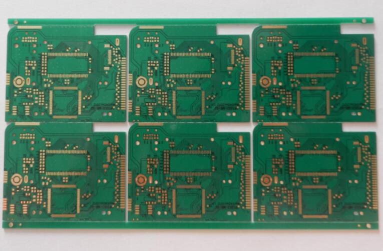
1. PCB board width ≤260mm (SIEMENS line) or ≤300mm (FUJI line); if semi-automatic dispensing is required, PCB board width*length ≤125mm*180mm.
2. The shape of the PCB board should be as close as possible to the square, not to form a Yin-Yang board.
3. The outer frame (clamping edge) of the PCB panel should be considered appropriate and a closed-loop preset should be used to ensure that the PCB panel is fixed on the fixture to ensure that it will not be deformed in the future.
4. The core distance between the small boards is controlled between 75mm and 145mm.
5. The connecting points between the outer frame of the jigsaw panel and the inner small board and the board should be attached to the nearest parts that must not be large or protruding parts, and there should be a space greater than 0.5mm between the components and the edge of the PCB board to ensure cutting The cutting tool is operating normally.
6. Four positioning holes are made at the four corners of the outer frame of the jigsaw panel, with an aperture volume of 4mm±0.01mm; the strength of the holes should be moderate to ensure that no disconnection occurs during the upper and lower boards; the precision of the aperture and position should be high. The wall of the hole is smooth and without burrs.

7. Each small board in the PCB jigsaw must have at least three positioning holes, 3≤aperture≤6mm, and no wiring or patching within 1mm of the edge positioning hole.
8. The reference symbols used for PCB positioning and fine-pitch component positioning. In principle, QFPs with a spacing of less than 0.65mm should be set at their diagonal positions; the positioning reference symbols used to form the PCB sub-board of the layout should be Used in pairs, placed at the opposite corners of the positioning elements.
9. When setting the reference positioning point, generally leave an unobstructed welding area 1.5mm larger than it around the positioning point.
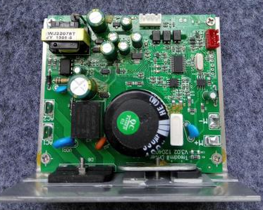
10. For large components, there are generally no more than 4 types of layout requirements. The number of layers, copper thickness, and appearance process requirements of each board are the same. In addition, consult with the engineers of the PCB manufacturer to obtain the most reasonable layout plan. .
Don't be too soft after the fight, try your best to ensure that there is enough support in the horizontal direction after the fight.
Moisture penetrates easily at the splicing.
After breaking it, use a file to smooth it.
Pay attention to the edges and slots when PCB is assembled.
The margins are for later soldering the plug-in or a fixed place for a moment, and the slotting is for the PCB board to be separated.
The process requirements for the margins are generally 2-4MM, and the components should be placed on the PCB board according to the maximum width.
Slotting means that the wiring layer is strictly prohibited, or the material layer. The specific agreement with the PCB manufacturer, the implementation of disposal and processing, and the pre-determined person in the position can indicate it.
Both v-groove and slotting are a form of milling profile. Multiple wrenches can be easily clutched when making a layout to prevent damage to the circuit board during clutching.
Determine which form to use based on the purely one-variety styles you put together into the layout. V-cut needs to go in a straight line and is not comfortable to fit the four wrenches of different sizes.
Panel size preset refers to the implementation of a little irregular and deformed PCB board to reduce the cost of PCB board. Joining PCB factory with experience in the processing of various process facilities, refer to the size of the board, and preset it to be suitable for the enterprise The layout size is assembled with the best board quality, the lowest production capital, the highest production rate, and the highest utilization rate of the board.
Finished unit size, nominal sample outside of the board, shape processing form, appearance handling form, number of spanner layers, finished board thickness, special processing requirements, etc.
Multi-layer board lamination form (main influencing factor), splicing on and off, pipe position form, experience in processing facilities in each process, shape processing form, etc.
Sheet size specifications, B sheet size specifications, dry die size specifications, RCC size specifications, copper foil size specifications, etc. provided by the board manufacturer.