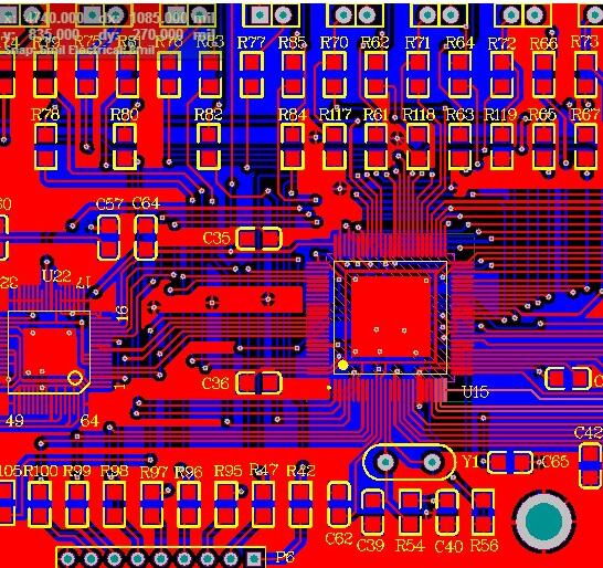
Step 1: Get a PCB board, first of all on the paper to record all the components of the model, parameters, and position, especially the diode, three machine tube direction, IC notch direction. It is best to take two pictures of the position of the ski with a digital camera.
Step 2: Remove all components and remove the tin from the PAD holes. Clean the PCB with alcohol, then put it in the scanner, start POHTOSHOP, color the screen screen and print it out for later use.

Step 3: Polish the TOP LAYER and BOTTOM LAYER slightly with water yarn paper until the copper film shines. Then put the two layers into the scanner, start PHOTOSHOP, and sweep the two layers in color respectively. Note that PCB must be placed horizontally and vertically in the scanner, otherwise the scanned image can not be used.
Step 4: Adjust the contrast and shade of the canvas, so that the part with copper film and the part without copper film contrast strongly, and then turn the picture to black and white, check whether the lines are clear, if not, repeat this step. If clear, save the picture as black and white BMP files top. BMP and bot.bmp.
Step 5: Convert the two BMP files into PROTEL files respectively, and transfer two layers into PROTEL. For example, the positions of PAD and VIA that have passed two layers basically coincide, indicating that the previous steps have been done well. If there is any deviation, repeat the third step.
Step 6: will TOP. BMP is converted to TOP. PCB, make sure to transfer to SILK layer, the yellow layer, then you trace the line on TOP layer, and place the device according to the drawing in step 2. Delete the SILK layer after painting.
Step 7: the BOT. BMP is converted to BOT. PCB, be sure to convert to SILK, the yellow layer, and then trace on the BOT layer. Delete the SILK layer after painting.
Step 8: Select TOP in PROTEL. PCB and BOT. PCB call in, combined into a picture is OK.
Step 9: Use laser printer to print the TOP LAYER and BOTTOM LAYER respectively to transparent film (1:1 ratio), put the film on that PCB, and compare whether there is any mistake.