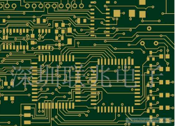
The process and function of PCB puzzle
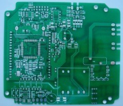
The size of a single PCB should be determined according to the overall structure of the whole machine. The size and shape of the PCB should be suitable for surface assembly production line production, in line with the size range of substrates applicable to printing machines and placement machines, and the working width of reflow soldering furnaces.
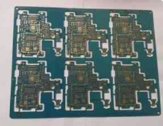
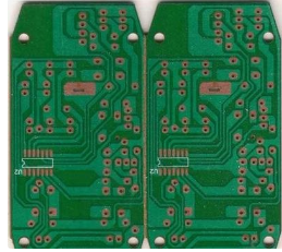
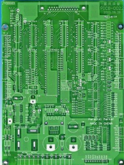
Due to the small size of SMB, in order to be more suitable for SMT automated production, multiple boards are often combined into one board, and several PCBs of the same unit are consciously combined into rectangles or squares, which is called puzzle board.

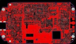
The use of splicing boards for small-sized PCBs can improve production efficiency, increase the applicability of the production line, and reduce tooling preparation costs. Single-sided mounting of the printed circuit board is mounted on the same side, and double-sided full mounting without wave soldering can use the double-numbered front and back sides of the board, and the graphics on both sides are arranged in the same way, this arrangement It can improve equipment utilization (each investment can be halved under the conditions of medium and small batch production), and save production preparation costs and time.
The pieces can be combined by V-groove linear division, stamp hole, punching and other technological means, which require accurate engraving, uniform depth, good mechanical support strength, but easy to be broken by the dividing machine or broken by hand.
The assembly of PCBs with small and identical printed circuits can also be carried out according to this principle, but attention should be paid to the method of compiling component tag numbers. Split printed circuit boards are commonly known as "stamp" boards.
(1) The stamp board can be composed of multiple same PCBs or multiple different PCBs.
(2) Determine the maximum dimensions of the stamp board according to the situation of the surface assembly equipment, such as the placement area of the placement machine, the maximum printing area of the printing machine and the working width of the reflow conveyor belt.
(3) The connecting ribs between the various circuit boards on the stamp board play the role of mechanical support. Therefore, it must have a certain strength and be easy to break to separate the circuit.
iPCB is a high-tech manufacturing enterprise focusing on the development and production of high-precision PCBs. iPCB is happy to be your business partner. Our business goal is to become the most professional prototyping PCB manufacturer in the world. Mainly focus on microwave high frequency PCB, high frequency mixed pressure, ultra-high multi-layer IC testing, from 1+ to 6+ HDI, Anylayer HDI, IC Substrate, IC test board, rigid flexible PCB, ordinary multi-layer FR4 PCB, etc. Products are widely used in industry 4.0, communications, industrial control, digital, power, computers, automobiles, medical, aerospace, instrumentation, Internet of Things and other fields.