What are the advantages and disadvantages of PCB spray tin plate?
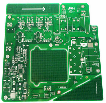
The spray tin board is a common type of PCB board, generally a multi-layer high-precision PCB board, which is widely used in various electronic equipment, communication products, computers, medical equipment, aerospace and other fields and products.
Tin spraying is a step and process flow in the production process of PCB board. Specifically, the PCB board is immersed in a molten solder pool, so that all exposed copper surfaces will be covered by solder, and then the hot air cutter is used to remove Remove the excess solder on the PCB board. Because the surface of the circuit board after tin spraying is the same substance as the solder paste, the soldering strength and reliability are better. However, due to its processing characteristics, the surface flatness of the tin spray treatment is not good, especially for small electronic components such as BGA package types. Due to the small welding area, if the flatness is not good, it may cause problems such as short circuits, so flatness is required. A better process to solve the problem of tin spraying board. Generally, the gold-plating process is selected (note that it is not a gold-plating process), and the principle and method of chemical displacement reaction are used for reprocessing, and a nickel layer with a thickness of 0.03~0.05um or about 6um is added to improve the surface flatness.
advantage:
1. The wettability is better during the soldering process of the components, and the soldering is easier.
2, it can prevent the exposed copper surface from being corroded or oxidized.

shortcoming:
is not suitable for soldering pins with fine gaps and components that are too small, because the surface flatness of the spray tin plate is poor. It is easy to produce solder bead during the processing of PCB manufacturers, and it is easy to cause short circuit to the fine pitch components. When used in the double-sided SMT process, because the second side has undergone a high-temperature reflow soldering, it is very easy to spray tin and re-melt, resulting in tin beads or similar droplets that are affected by gravity into spherical tin dots, which will cause the surface to be even worse. Flattening affects welding problems.
With the advancement of technology, PCB proofing in the industry now has a tin spraying process suitable for assembling QFP and BGA with a smaller pitch, but there are fewer practical applications. At present, some PCB proofing uses OSP process and gold immersion process to replace the tin spraying process; technological developments have also led some factories to adopt tin and silver immersion processes. In addition to the lead-free trend in recent years, the use of the tin spraying process has been further limit.
At present, the country has higher and higher requirements for environmental protection and greater efforts in link governance. This is a challenge but also an opportunity for PCB factories. If PCB factories are determined to solve the problem of environmental pollution, then FPC flexible circuit board products can be at the forefront of the market, and PCB factories can get opportunities for further development.
The Internet era has broken the traditional marketing model, and a large number of resources have been gathered together to the greatest extent through the Internet, which has also accelerated the development speed of FPC flexible circuit boards, and then as the development speed accelerates, environmental problems will continue to appear in PCB factories. In front of him. However, with the development of the Internet, environmental protection and environmental informatization have also been developed by leaps and bounds. Environmental information data centers and green electronic procurement are gradually being applied to the actual production and operation fields. From this point of view, the environmental protection problems of PCB factories can be solved from the following two points.