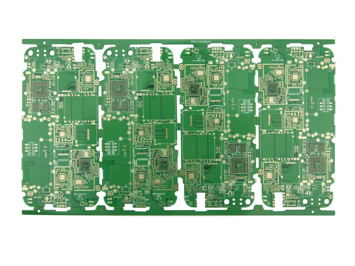
In the process of finding and placing components on the PCB board, PCB proofing can save you time by cross-selecting component layouts. Have you had such an experience? I wasted a lot of time searching for a certain component on the circuit board, and finally found that it was hidden in a completely different position in your schematic design? Cross-select component layout, you can select specific components in an orderly manner on the schematic, and then place them in an orderly manner on the PCB board. This keeps your design organized and easy to edit.

Cross-select component layout
PCB design cross-select component layout
Cross selection and component placement between schematic and PCB
how to use
You don't have to change the view settings to cross-select or move components. This is useful when splitting the schematic and board work space horizontally or vertically to match the schematic and PCB layout. To cross-select components:
1. Hold down the Shift key, and click on all the components you want to place on the circuit board on the schematic.
2. Switch to the PCB document, select Tools》 Component Placement》 ReposiTIon Selected Components.
3. Click the PCB board to place the selected components.
The components placed on the PCB will follow the order selected in the schematic, so as to maintain the consistency and coordination of the design.
Component cutting line
PCB design cross-select component layout
Add components to existing wires
We all want to edit the design in the fastest way. A common modification in the design is to add components to an existing network connection. A tedious and lengthy method is to delete the line segments, add components, and then reconnect the two sides of the components.
Another more effective and productive method is to use the component cutting line function in the DXP setting. In this way, you can place components on existing wires, and the wires will be automatically cut without overlapping the components. Compared with the first method, this saves a lot of time!