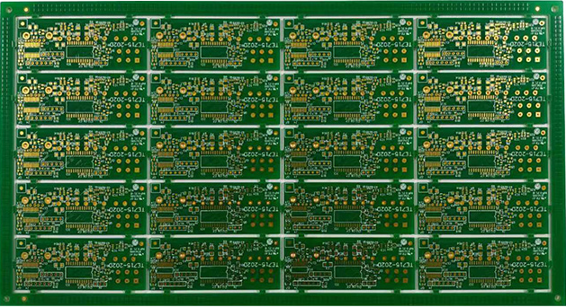
Printed Circuit Board (PCB), also known as circuit board, PCB board, aluminum substrate, high frequency board, ultra-thin circuit board, ultra-thin circuit board, printed (copper etching skills) circuit board, etc., is important Electronic components are the support of electronic components and the provider of circuit connection of electronic components. The traditional circuit board uses the method of printing etching resist to make the circuit lines and drawings, so it is called a printed circuit board or a printed circuit board. As electronic products continue to be miniaturized and refined, most of the circuit boards now choose to attach etching resists (laminated or coated), and after exposure and development, the circuit boards are made by etching.
2. Circuit board principle-structure
The circuit board is mainly composed of pads, vias, device holes, wires, components, connectors, fillers, electrical gaps, etc. Common layer structures include single layer PCB, double layer PCB, and multi layer PCB. The main functions of each component are as follows:

Pad: A metal hole used to solder the pins of components.
Via: There are metal vias and non-metal vias, and the metal vias are used to connect the pins of components between each layer.
Device hole: used to fix the circuit board.
Wire: The copper film of the electrical network used to connect the pins of the components.
Connectors: components used to connect between circuit boards.
Filling: used for the copper coating of the ground wire network, which can effectively reduce the impedance.
Electrical gap: used to determine the size of the circuit board, all components on the circuit board cannot exceed the gap.
3. Circuit board principle
The working principle of the circuit board: is to use the board-based insulating material to separate the conductive layer of the outer copper foil, so that the current is completed along the pre-planned path in various components such as work, amplification, attenuation, modulation, demodulation, and coding And other functions.
On the most basic PCB, the parts will be gathered on one side, and the wires will be gathered on the other side. Since the wires only appear on one side in between, this kind of PCB is called a single panel. For multi-layer boards, multiple layers have wires. It is necessary to have a proper circuit connection between the two layers. The bridge between such circuits is called a via. The fundamental planning process of the circuit board can be divided into the following four processes:
(1) The planning of the schematic circuit diagram---The planning of the schematic circuit diagram mainly uses the schematic diagram editor of Protel DXP to make the schematic diagram.
(2) Generate a network report---The network report is a report that shows the link between the circuit principle and each component in the report. It is the bridge and tie connecting the circuit schematic plan and the circuit board planning, and the network report through the circuit schematic diagram, Can quickly find the connection between the components, so as to provide convenience for the subsequent PCB planning.
(3) The planning of the printed circuit board-the planning of the printed circuit board is what we generally call the PCB planning. It is the final way to transform the circuit schematic diagram. This part of the related planning is larger than the circuit schematic plan. We can use the powerful planning function of Protel DXP to complete this part of the planning.
(4) Generate printed circuit board reports---After the printed circuit board planning is completed, various reports need to be generated, such as pin reports, circuit board information reports, network status reports, etc., and finally printed circuit diagrams are printed out.