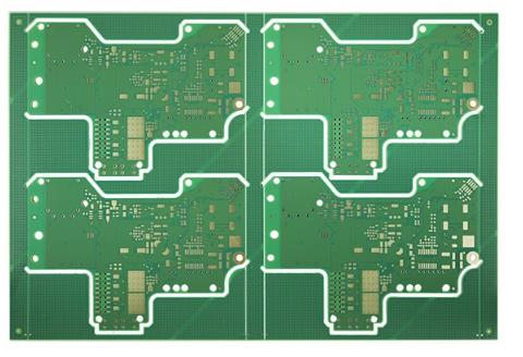
High-speed PCB design needs to pay attention to the following issues:
1. The influence of wiring topology on signal integrity
Signal integrity problems may arise when signals are transmitted along transmission lines on high-speed PCB boards. Netizen tongyang of STMicroelectronics asked: For a set of buses (address, data, commands) driving up to 4 or 5 devices (FLASH, SDRAM, etc.), when PCB wiring, the bus arrives at each device in turn, as first Connect to SDRAM, then to FLASH...The bus is still distributed in a star shape, that is, it is separated from a certain place and connected to each device. These two methods are in terms of signal integrity.
The impact of PCB wiring topology on signal integrity is mainly reflected in the inconsistent signal arrival time at each node, and the reflected signal also arrives at a certain node at inconsistent time, which causes the signal quality to deteriorate. Generally speaking, the star topology structure can make the signal transmission and reflection delays consistent by controlling several branches of the same length to achieve better signal quality. Before using the topology, the situation of the signal topology node, the actual working principle and the wiring difficulty should be considered.

Different buffers have different effects on signal reflection, so the star topology cannot solve the delay of the data address bus connected to FLASH and SDRAM, and thus cannot ensure the quality of the signal; on the other hand, high-speed signals generally For communication between DSP and SDRAM, the rate of FLASH loading is not high, so in high-speed simulation, only the waveform at the node where the actual high-speed signal works effectively is ensured, instead of paying attention to the waveform at FLASH; star topology is compared with daisy chain and other topologies. In other words, wiring is more difficult, especially when a large number of data address signals use star topology.
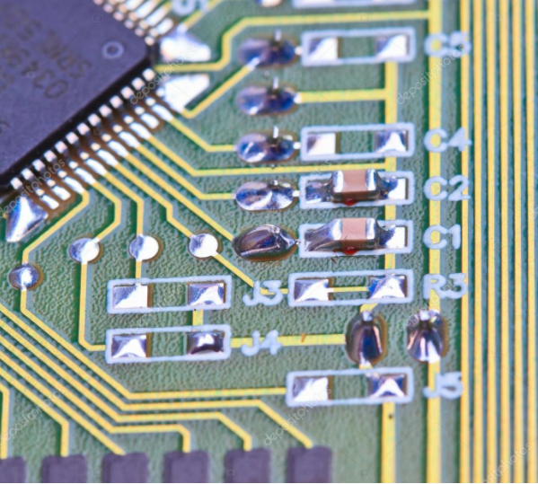
2. The impact of pads on high-speed signals
In the PCB, from a design point of view, a via is mainly composed of two parts: the middle hole and the pads around the hole. An engineer named fulonm asked the guest about the impact of pads on high-speed signals. In this regard, Li Baolong said: pads have an impact on high-speed signals, and it affects the impact of similar device packaging on devices. A detailed analysis shows that after the signal comes out of the IC, it passes through the bonding wire, pins, package shell, pad, and solder to the transmission line. All joints in this process will affect the quality of the signal. But in actual analysis, it is difficult to give the specific parameters of the pad, solder and pin. Therefore, the package parameters in the IBIS model are generally used to summarize them. Of course, such analysis can be received at lower frequencies, but for higher frequency signals, higher-precision simulations are not accurate enough. A current trend is to use IBIS's V-I and V-T curves to describe buffer characteristics, and to use SPICE models to describe package parameters.
3. How to suppress electromagnetic interference
PCB is the source of electromagnetic interference (EMI), so PCB design is directly related to the electromagnetic compatibility (EMC) of electronic products. If emphasizing EMC/EMI in high-speed PCB design, it will help shorten the product development cycle and speed up the time to market. Therefore, many engineers are very concerned about the problem of suppressing electromagnetic interference in this forum. For example, Shu Jian of Wuxi Xiangsheng Medical Imaging Co., Ltd. said that the harmonics of the clock signal were found to be very serious in the EMC test. Is it necessary to perform special treatment on the power supply pins of the IC that uses the clock signal? Connect a decoupling capacitor to the power supply pin. What aspects should be paid attention to in PCB design to suppress electromagnetic radiation? In this regard, Li Baolong pointed out that the three elements of EMC are radiation source, transmission route and victim. The propagation path is divided into space radiation propagation and cable conduction. So to suppress harmonics, first look at the way it spreads. Power supply decoupling is to solve the propagation of conduction mode. In addition, necessary matching and shielding are also required.
Filtering is a good way to solve EMC radiation through conduction. In addition, it can also be considered from the aspects of interference sources and victims. In terms of interference sources, try to use an oscilloscope to check whether the signal rising edge is too fast, there is reflection or overshoot, undershoot or ringing. If so, you can consider matching; in addition, try to avoid making 50% duty cycle signals, because this kind of signal has no even There are more sub-harmonics and more high-frequency components. For the victims, measures such as land coverage can be considered.
Four, RF wiring is to choose via or bend wiring
Analyzing the return path of the RF circuit is not the same as the return path of the signal in the high-speed digital circuit. The two have something in common, both are distributed parameter circuits, and both use Maxwell's equation to calculate the characteristics of the circuit. However, the radio frequency circuit is an analog circuit, in which the voltage V=V(t) and current I=I(t) both need to be controlled, while the digital circuit only pays attention to the change of signal voltage V=V(t). Therefore, in RF wiring, in addition to considering signal return, it is also necessary to consider the influence of wiring on current. That is, whether the bending of the wiring and the via has any effect on the signal current. In addition, most RF boards are single-sided or double-sided PCBs, and there is no complete plane layer. The return paths are distributed on various grounds and power supplies around the signal. 3D field extraction tools are required for analysis during simulation. The reflow of vias requires specific analysis; high-speed digital circuit analysis generally only deals with multi-layer PCBs with complete plane layers, using 2D field extraction analysis, and only considers signal reflow in adjacent planes. Vias are only used as a lumped parameter RLC deal with.