Most of the circuit boards are prone to board bending and warping during reflow soldering. In severe cases, it may even cause components such as empty soldering and tombstones. How to overcome these problems? Why is the PCB board deformed? Are there any measures to improve PCB board deformation?
The hazards of PCB board deformation
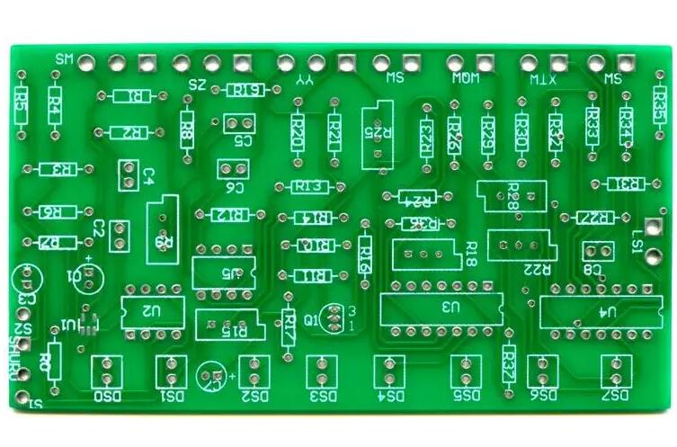
In the automated surface mount line, if the circuit board is not flat, it will cause inaccurate positioning, components cannot be inserted or mounted on the holes and surface mount pads of the board, and even the automatic insertion machine will be damaged. The circuit board on which the components are installed is bent after soldering, and the component feet are difficult to cut neatly. The board cannot be installed on the chassis or the socket inside the machine, so it is also very annoying for the assembly plant to encounter the board warping. The current surface mount technology is developing in the direction of high precision, high speed, and intelligence, which puts forward higher flatness requirements for PCB boards that are home to various components.

In the IPC standard, it is specifically pointed out that the maximum allowable deformation of PCB boards with surface mount devices is 0.75%, and the maximum allowable deformation of PCB boards without surface mounting is 1.5%. In fact, in order to meet the requirements of high-precision and high-speed placement, some electronic assembly manufacturers have stricter requirements for deformation. For example, our company has multiple customers who require a maximum deformation of 0.5%, and even some customers require it. 0.3%.
The PCB board is composed of copper foil, resin, glass cloth and other materials. The physical and chemical properties of each material are different, and thermal stress will inevitably occur after being pressed together, which will cause deformation. At the same time, in the PCB processing process, it will go through various processes such as high temperature, mechanical cutting, wet treatment, etc., which will also have an important impact on the deformation of the board. In short, the reasons for the deformation of the PCB can be complex and diverse. How to reduce or eliminate the material characteristics Distortion or deformation caused by processing has become one of the most complicated problems faced by PCB manufacturers.
Analysis of the causes of PCB board deformation
Generally, a large area of copper foil is designed on the circuit board for grounding purposes. Sometimes there is also a large area of copper foil designed on the Vcc layer. When these large area copper foils cannot be evenly distributed on the same circuit board When it is installed, it will cause uneven heat absorption and heat dissipation. Of course, the circuit board will also expand and contract. If the expansion and contraction cannot be done at the same time, it will cause different stress and deformation. At this time, if the temperature of the board has reached At the upper limit of the Tg value, the board will begin to soften, causing permanent deformation.
The connection points (vias, vias) of each layer on the circuit board will limit the expansion and contraction of the board
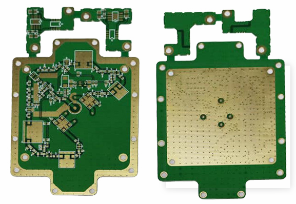
Today's circuit boards are mostly multi-layer boards, and there will be rivet-like connection points (vias) between the layers. The connection points are divided into through holes, blind holes and buried holes. Where there are connection points, the board will be restricted. The effect of expansion and contraction will also indirectly cause plate bending and plate warping.
The weight of the circuit board itself will cause the board to dent and deform
Generally, the reflow furnace uses a chain to drive the circuit board forward in the reflow furnace, that is, the two sides of the board are used as fulcrums to support the entire board. If there are heavy parts on the board, or the size of the board is too large, It will show a depression in the middle due to the amount of seed, causing the plate to bend.
The depth of the V-Cut and the connecting strip will affect the deformation of the jigsaw
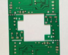
Basically, V-Cut is the culprit that destroys the structure of the board, because V-Cut cuts grooves in the original large sheet, so the V-Cut is prone to deformation. (Related reading: Circuit board to the board edge-V-Cut sub-board machine)
Improvement measures for PCB deformation
1. Reduce the effect of temperature on the stress of the board
Since "temperature" is the main source of board stress, as long as the temperature of the reflow furnace is lowered or the rate of heating and cooling of the board in the reflow furnace is slowed, the occurrence of plate bending and warpage can be greatly reduced. But there may be other side effects.
2. Use high Tg plates
Tg is the glass transition temperature, that is, the temperature at which the material changes from the glass state to the rubber state. The lower the Tg value of the material, the faster the board starts to soften after entering the reflow oven, and the time it takes to become soft rubber state It will also become longer, and the deformation of the board will of course be more serious. Using a higher Tg plate can increase its ability to withstand stress and deformation, but the price of the material is relatively high.
3. Increase the thickness of the circuit board
In order to achieve the purpose of lighter and thinner for many electronic products, the thickness of the board has left 1.0mm, 0.8mm, or even 0.6mm. Such a thickness must keep the board from deforming after the reflow furnace, which is really difficult. It is recommended that if there is no requirement for lightness and thinness, the thickness of the board should be 1.6mm, which can greatly reduce the risk of bending and deformation of the board.
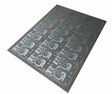
4. Reduce the size of the circuit board and reduce the number of puzzles
Since most of the reflow furnaces use chains to drive the circuit board forward, the larger the size of the circuit board will be due to its own weight, dent and deformation in the reflow furnace, so try to put the long side of the circuit board as the edge of the board. On the chain of the reflow furnace, the depression and deformation caused by the weight of the circuit board can be reduced. The reduction in the number of panels is also based on this reason. That is to say, when passing the furnace, try to use the narrow edge to pass the furnace direction as far as possible to achieve the lowest The amount of depression deformation.
5. Used furnace tray fixture
If the above methods are difficult to achieve, the last is to use reflow carrier/template to reduce the amount of deformation. The reason why the reflow carrier/template can reduce the bending of the plate is because whether it is thermal expansion or cold contraction, it is hoped The tray can hold the circuit board and wait until the temperature of the circuit board is lower than the Tg value and start to harden again, and can also maintain the size of the garden.
If the single-layer pallet cannot reduce the deformation of the circuit board, a cover must be added to clamp the circuit board with the upper and lower pallets. This can greatly reduce the problem of circuit board deformation through the reflow furnace. However, this furnace tray is quite expensive, and manual labor is required to place and recycle the trays.
6. Use real connections and stamp holes instead of V-Cut sub-boards
Since V-Cut will destroy the structural strength of the panel between the circuit boards, try not to use the V-Cut sub-board or reduce the depth of the V-Cut.