One aspect of the cause of warpage of the printed circuit board is that the PCB substrate (copper clad laminate) used may warp, but during the processing of the printed circuit board, thermal stress, chemical factors, and improper production technology can also cause The printed circuit board warps.
Therefore, for the printed circuit board factory, the first thing is to prevent the printed circuit board from warping during the processing; the second is to have a suitable and effective treatment method for the PCB boards that has already warped.
1. Prevent printed circuit board from warping during processing
1. Prevent or increase the warpage of the substrate due to improper inventory method
(1) Since the copper clad laminate is in the storage process, because moisture absorption will increase the warpage, the moisture absorption area of the single-sided copper clad laminate is large. If the inventory environment humidity is high, the single-sided copper clad laminate will significantly increase the warpage. The moisture of double-sided copper clad laminate can only penetrate from the end surface of the product, the moisture absorption area is small, and the warpage changes slowly. Therefore, for the copper clad laminates without moisture-proof packaging, attention should be paid to the warehouse conditions, minimize the humidity in the warehouse and avoid bare copper clad laminates to avoid increased warpage of the copper clad laminates in storage.

(2) Improper placement of copper clad laminates will increase warpage. Such as vertical placement or heavy objects on the copper clad laminate, improper placement, etc. will increase the warpage and deformation of the copper clad laminate.
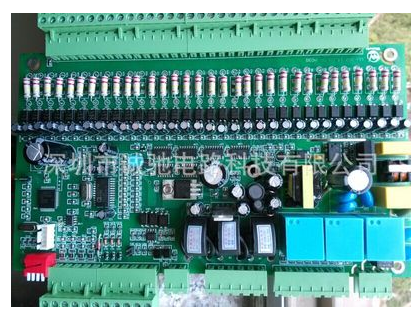
Soldered PCBA
2. Avoid warping caused by improper printed circuit board circuit design or improper processing technology.
For example, the conductive circuit pattern of the PCB boards is not balanced or the PCB
The lines on both sides of the board are obviously asymmetrical, and there is a large area of copper on one side, which forms a large stress, which makes the PCB board warp. The high processing temperature or large thermal shock in the PCB manufacturing process will cause the PCB board to warp. As for the impact caused by improper storage method of superstrate, PCB factory is better to solve it, and it is enough to improve the storage environment and eliminate vertical placement and avoid heavy pressure. For PCB boards with a large area of copper in the circuit pattern, it is best to mesh the copper foil to reduce stress.
3. Eliminate substrate stress and reduce PCB boards warpage during processing
In the process of PCB processing, the substrate has to be subjected to heat and many kinds of chemical substances many times. For example, after the substrate is etched, it needs to be washed, dried and heated. Electroplating is hot during pattern plating. After printing green oil and marking characters, it must be heated or dried with UV light. Thermal shock to the substrate when hot air is sprayed. It's also very big and so on. These processes may cause the PCB board to warp.
4. When wave soldering or dip soldering, the solder temperature is too high and the operation time is too long, which will increase the warpage of the substrate. For the improvement of the wave soldering process, the electronic assembly factory needs to cooperate.
Since stress is the main cause of substrate warpage, if the copper clad laminate (also called h board) is baked before the copper clad laminate is put into use, many PCB manufacturers believe that this approach is beneficial to reduce the warpage of the PCB boards. The function of the baking sheet is to fully relax the stress of the substrate, thereby reducing the warpage and deformation of the substrate during the PCB manufacturing process.
The method of board is: conditional PCB factories use large oven h board. Put a large stack of copper clad laminates into the oven before production, and bake the copper clad laminates for several to ten hours at a temperature near the glass transition temperature of the substrate. The PCB boards produced by the copper clad laminate of the h board has relatively small warpage deformation, and the product qualification rate is much higher. For some small PCB factories, if there is no such large oven, the substrate can be cut into small pieces and then bake, but there should be a heavy object to press the plate when baking the plate, so that the substrate can be kept flat during the stress relaxation process. The temperature of the baking sheet should not be too high, because the substrate will change color if the temperature is too high. It should not be too low, and it takes a long time for the temperature to be too low to relax the substrate stress.